
Every load and store in an SoC carries an address, and something in the chip must decide which block that address belongs to. The memory map is the plan that assigns address ranges to blocks, and address decoding is the hardware that carries the plan out on every access. Both look simple, and both are a common source of integration bugs: overlapping ranges, holes nobody answers, registers that appear at several addresses at once. This article explains how architects lay out a memory map, how decoding works level by level in real hardware, what full and partial decoding mean, and shows with a simulation that a partially decoded block really does answer at addresses it was never meant to own.
13 min read | Beginner to Intermediate
What You'll Learn
- Lay out a memory map with aligned power-of-two regions and room to grow
- Explain how decoders turn an address into a block select, level by level
- Distinguish full and partial decoding, and predict aliases
- Connect the hardware memory map to the linker script and the software headers
The Address Space and the Map
A 32-bit processor can name 232 byte addresses, 4 GB, its address space. Even a large SoC uses only part of it. The memory map lists which ranges are owned, by which block, and what happens everywhere else. In a small example SoC it looks like this:
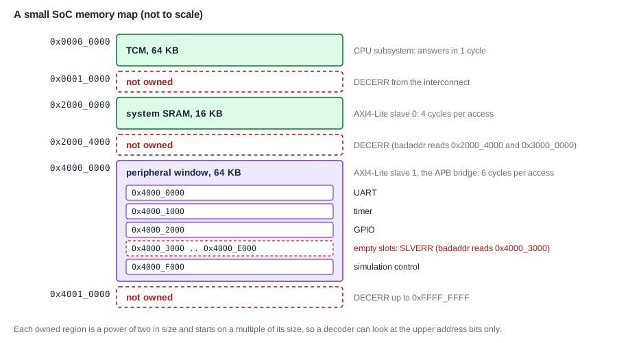
| Region | Range | Size | Owner |
|---|---|---|---|
| TCM | 0x0000_0000 to 0x0000_FFFF | 64 KB | CPU subsystem (local, no bus) |
| system SRAM | 0x2000_0000 to 0x2000_3FFF | 16 KB | SRAM, through the interconnect |
| peripheral window | 0x4000_0000 to 0x4000_FFFF | 64 KB | APB bridge, 16 slots of 4 KB |
| UART, timer, GPIO, simulation control | 0x4000_0000, 0x4000_1000, 0x4000_2000, 0x4000_F000 | 4 KB each | slots 0, 1, 2 and F |
| everything else | - | - | nobody: an error response |
The layout is not arbitrary. Code memory at the bottom, on-chip SRAM at 0x2000_0000 and peripherals at 0x4000_0000 is the same split as the standard address map of Arm's Cortex-M microcontroller architecture, which many tools and programmers know. Following a familiar convention costs nothing and avoids surprises.
Laying Out a Map
Architects follow a few rules when they assign addresses.
Powers of Two, Aligned to Their Size
Every region has a size that is a power of two, and starts at an address that is a multiple of that size. The SRAM is 16 KB and starts at 0x2000_0000, a multiple of 16 KB; each peripheral slot is 4 KB and starts at a multiple of 4 KB. Then a region is defined by its upper address bits alone. All addresses of the 64 KB peripheral window have the same bits 31 to 16, 0x4000, and differ only in bits 15 to 0. Deciding whether an address is in the window is a 16-bit equality test, and the lower 16 bits pass through to the block unchanged as its internal offset.
A region that broke this rule, say 24 KB starting at 0x2000_1000, would need a comparison of the address against both a lower and an upper bound, which is larger and slower logic, and its blocks could not use the address bits directly as offsets. Memory protection hardware usually expects the same alignment: RISC-V's physical memory protection, for example, has a compact way to describe naturally aligned power-of-two regions.
Group by Kind and Leave Gaps
Memories, peripherals and special regions are grouped, so that a decoder can separate them with a few high address bits, and so that rules such as "peripherals are never cached" apply to whole ranges. Between regions, the map leaves reserved space. The SRAM region could grow from 16 KB to 512 MB before reaching the peripherals at 0x4000_0000; the peripheral window has 12 empty slots. The next version of the chip can add memory or blocks without moving anything that existing software depends on. Moving a block's address breaks every driver that uses it, so maps are designed for growth from the first version.
Quick Check
Q: A designer wants to add a 32 KB SRAM. Which of the base addresses 0x2000_4000, 0x2000_8000 and 0x3000_0000 satisfy the alignment rule?
Show Answer
32 KB is 0x8000. 0x2000_8000 and 0x3000_0000 are multiples of 0x8000; 0x2000_4000 is not, so a 32 KB region there would straddle a 32 KB boundary. 0x2000_8000 keeps the SRAMs together, leaving 0x2000_4000 to 0x2000_7FFF free; 0x3000_0000 starts a new group.
Decoding, Level by Level
An address decoder compares an address with the map and produces a select signal for the block that owns it. In an SoC, decoding happens in several levels, each one looking at a different part of the address. Here is the path of a read of 0x4000_2008 in the small SoC:
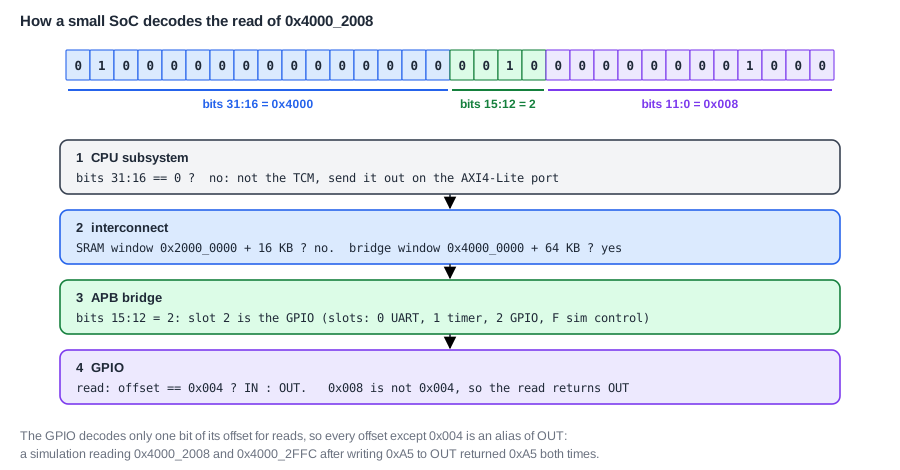
- CPU subsystem. It checks whether bits 31 to 16 are all zero. If so, the address is in the 64 KB TCM and never leaves the subsystem. 0x4000_2008 is not, so it goes out on the AXI4-Lite port.
- Interconnect. It holds a base and a size for each subordinate and checks each one: is the address at least the base and less than base + size? The SRAM window does not match; the bridge window, 0x4000_0000 plus 64 KB, does. Because the windows are aligned powers of two and the bases are constants, synthesis can reduce these comparisons to equality tests on the upper bits.
- APB bridge. It uses bits 15 to 12 to choose one of up to 16 peripheral slots. Here they are 2, the GPIO.
- Peripheral. The GPIO uses the remaining offset, bits 11 to 0, to choose a register.
If no subordinate matches at the interconnect, it answers the access itself with a decode error (DECERR); if the bridge's slot is empty, the bridge answers with a slave error (SLVERR). Every access gets an answer, so a wrong address cannot hang the chip. Buses and Transactions measures those error responses.
Decoding in levels keeps each decoder small. The interconnect does not need to know about individual peripheral registers, and the peripherals do not need to know where in the address space they live: each one sees only its 12-bit offset. The same UART block could be placed in any slot, or in another chip, without changing its RTL.
Full and Partial Decoding
A decoder that checks every address bit that could distinguish two locations is fully decoding. One that checks only some of them is partially decoding, and then one location answers at several addresses, which are called aliases.
The GPIO in this SoC is an example. It has two registers, OUT at offset 0x000 and IN at offset 0x004. Its read multiplexer checks a single condition: if the offset is 0x004, return IN; otherwise return OUT. Every one of the other 1,023 word offsets in its 4 KB slot therefore reads as OUT. The UART, by contrast, decodes its full offset and returns 0 for any offset that is not one of its registers.
That is a prediction from the RTL, so it was tested in simulation. A small program writes 0xA5 to OUT, then reads the GPIO at offsets 0x008 and 0xFFC, reads OUT itself, and reads an unused UART offset, 0x00C.
All four predictions held: 0x4000_2008 and 0x4000_2FFC both returned 0xA5, the value of OUT, and the unused UART offset returned 0, with no bus errors. As far as software can tell, the GPIO's OUT register exists at more than a thousand addresses.
Why Partial Decoding Exists, and Why It Is Risky
Partial decoding saves logic: the GPIO needs one comparison instead of a full check of the offset. In small and cost-sensitive designs, and in older systems built from separate chips, it was common. Its risk is that software can use an alias by mistake, for example through a wrong offset in a driver, and the code works. When the next version of the chip adds a register at that offset, or decodes fully, the driver breaks. Modern specs therefore usually require full decoding, or at least state exactly which addresses alias, and define that unused offsets read as zero and ignore writes.
Where Does This Matter?
Memory-map bugs are among the first things SoC verification checks: every register of every block is read and written at its address, and unused addresses are checked for the specified response. Automatic register tests, generated from the same description as the RTL, write each register and read it back, and check that writing one register does not change another, which is how aliases and overlapping windows are caught before silicon.
Several Managers, Several Views
In a system with more than one manager, every manager needs its own view of the map. A DMA engine must reach the memories and the peripherals it feeds, but usually not the processor's private TCM; a display controller needs only DRAM. The interconnect's decoders define which subordinates each manager can reach. Addresses that one manager can use may be unowned for another, and it must still get an error response rather than hang.
Most systems keep the same address for the same block in every manager's view, so that software can pass a buffer's address to a DMA engine without converting it. Where views differ, for example when a processor's local memory is visible to others at a different, global address, the spec must state both addresses, and drivers must convert between them.
Remapping at Boot
Some chips change the map at run time. A common case is the boot alias: after reset, the boot ROM appears at address 0, where the processor starts, and also at its normal address. Once the boot code has copied what it needs into RAM, it writes a control register that remaps address 0 to RAM, so that the interrupt vectors and the program can live there. Remapping is a deliberate, documented alias, controlled by software; the decoders simply choose between two targets for the same range depending on that register. Boot ROM and the Boot Flow describes what happens before that point.
The Map in Software
Software has its own copy of the memory map in two places. The linker script tells the linker where code and data go. In the small SoC it places everything, code, constants, variables, at address 0 onward, in the TCM, and the start-up code puts the stack at 0x1_0000, the top of the TCM. A C header file defines the base address of each device, SRAM_BASE 0x20000000u, UART_BASE 0x40000000u and so on, and drivers build every register address from those. If the hardware map changes and these two files do not, the software silently writes to the wrong place, which is why they are generated from the same source as the hardware where possible. The System Architecture Spec describes that practice.
Quick Check
Q: A program on the small SoC reads 0x4000_2004 and 0x4000_2804. What does each read return?
Show Answer
Both are in the GPIO slot. 0x4000_2004 has offset 0x004, so it returns IN, the input pins. 0x4000_2804 has offset 0x804, which is not 0x004, so the partial decoder returns OUT. They look similar but read different registers.
Common Mistakes
Mistake #1: Overlapping windows
If two subordinates' windows overlap, an address selects both, and depending on the interconnect either one wins silently or both respond and the bus breaks. Check every map for overlaps, ideally automatically from the description.
Mistake #2: Unaligned or odd-sized regions
A region that is not a power of two or not aligned to its size needs larger comparators, cannot pass its address bits straight through as offsets, and is hard to protect. Round sizes up and align them.
Mistake #3: Relying on aliases
Code that works only because a block partially decodes its addresses breaks when the decoder changes. Use the documented address of every register, and specify unused offsets in the spec.
Practice Exercise
Challenge: Who Answers?
For each read on the small SoC, say which block answers and what the response is: (a) 0x2000_3FFC; (b) 0x2000_4000; (c) 0x3000_0000; (d) 0x4000_3000; (e) 0x4000_2010 after OUT was written with 0x55; (f) 0x4001_0000.
Hint
Check the levels in order: TCM (bits 31:16 zero), interconnect windows, bridge slots, and finally the peripheral's own decoding.
Solution
(a) The SRAM, OKAY: it is the last word of the 16 KB window 0x2000_0000 to 0x2000_3FFF. (b) The interconnect, DECERR: the first byte after the SRAM window, owned by nobody. (c) The interconnect, DECERR: a gap in the map. (d) The APB bridge, SLVERR: inside the peripheral window, but slot 3 is empty. (e) The GPIO, OKAY, data 0x55: offset 0x010 is not 0x004, so the partial decoder returns OUT. (f) The interconnect, DECERR: 0x4001_0000 is just past the 64 KB peripheral window.
Summary
- The memory map assigns address ranges to blocks; the small example SoC places its TCM, SRAM and peripherals at 0x0000_0000, 0x2000_0000 and 0x4000_0000, like the Cortex-M convention.
- Regions are powers of two aligned to their size, grouped by kind, with reserved space to grow.
- Decoding happens in levels: CPU subsystem, interconnect windows, bridge slots, then each block's offset; unowned addresses get DECERR or SLVERR.
- Partial decoding creates aliases: a simulation confirmed that the GPIO's OUT register answers at 0x4000_2008 and 0x4000_2FFC.
- The linker script and device headers are the software copy of the map, and must change with the hardware.
