
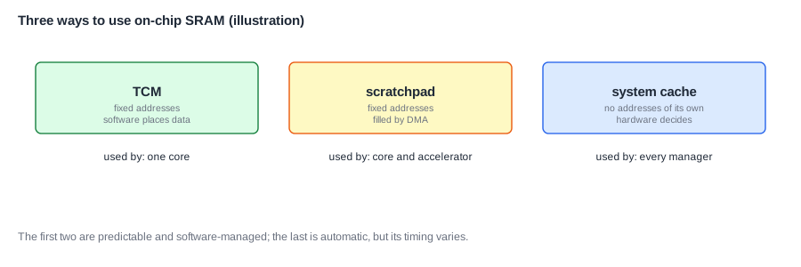
On-chip SRAM is the fastest memory an SoC has outside the processors' own caches, and the most expensive per bit. How it is used is a design decision with several good answers: as a tightly coupled memory for one core, as a scratchpad shared by a core and an accelerator, or as a system cache in front of DRAM that every block can use. This article explains each role, how a system cache differs from a processor cache, how to decide how much SRAM to spend and where, and the costs that come with each choice.
12 min read | Intermediate
What You'll Learn
- Compare TCMs, scratchpads and system caches
- Explain how a system cache reduces DRAM traffic and power
- Describe how system caches are partitioned between clients
- Decide how much on-chip SRAM to spend, and where
Why On-Chip SRAM
Memories in a System showed that SRAM is fast but large. In one estimate in an older 130 nm process, a 64 KB memory built from SRAM blocks was about 91 times the area of a small processor core. Every kilobyte must earn its place. It does so in three ways: by being faster than DRAM, by using far less energy per access than going off chip, and by making timing predictable. The three main roles each use these benefits differently.
Tightly Coupled Memory
A TCM is SRAM attached directly to one core, at a fixed range of addresses. Software decides what goes there, usually through the linker. It answers in a cycle or two, every time, with no misses. That makes it ideal for code and data with hard timing requirements: interrupt handlers, control loops, stacks. Integrating the CPU Subsystem describes how a core reaches it. In one small SoC, a copy routine ran about 22 percent slower with its buffer in a shared SRAM than with the buffer in the TCM.
Its limitation is that it serves one core and holds only what software put there. If the data doesn't fit, software must move it in and out, by hand or with DMA.
Scratchpads
A scratchpad is also SRAM at fixed addresses, but shared between several blocks, often a processor and an accelerator, or several stages of a pipeline. A DMA engine fills it with the next piece of work while the accelerator processes the current one, using two buffers in turn, a scheme called double buffering. The accelerator's timing is fully predictable, and DRAM is touched only for the bulk transfers, in efficient bursts.
Scratchpads are common in DSPs, image processors and machine learning accelerators, whose access patterns are known in advance. Software, or a compiler, plans exactly what goes into the scratchpad and when. That planning is the cost: it is hard work, and it must be redone for every new algorithm. In return, a scratchpad avoids the tags, the comparison logic and the unpredictable misses of a cache, so it delivers more data per square millimeter and per joule.
Quick Check
Q: An accelerator processes images in 32 KB tiles, each taking 50 µs. A DMA engine can move a tile in 30 µs. How does double buffering keep the accelerator busy, and how much scratchpad does it need?
Show Answer
While the accelerator works on one tile, the DMA engine loads the next into the other buffer. Loading takes 30 µs, less than the 50 µs of processing, so the next tile is always ready. It needs two 32 KB buffers, 64 KB, plus space for results if they are written out the same way.
System Caches
A system cache, sometimes called a last-level cache or system-level cache, sits in front of the memory controller and is shared by all the managers on the chip: CPUs, GPU, display, camera, accelerators. It has no addresses of its own. It keeps copies of recently used DRAM data, and hardware decides what to keep, exactly like a processor cache, as Cache Organization explains. Any block that reads data still in the system cache gets it without a DRAM access.
Its benefits are different from a processor cache's. It is often not much faster than DRAM for a single access, after the long trip across the interconnect. Its main value is reducing DRAM traffic, and so DRAM power and bandwidth use. Data passed from one block to another, such as a frame written by the GPU and read by the display, can stay in the system cache and never go off chip. That can cut a large part of the traffic in a budget, as Memory Bandwidth Budgets explains.
Sharing It Fairly
A shared cache has a classic problem: one client can push out everyone else's data. A GPU streaming through large textures could fill the cache with data used once, and evict the CPU's working set. So system caches are usually partitioned. Each client, or group, gets an ID on its transactions, and the cache allocates a certain number of ways, or a certain capacity, to each ID. A streaming client can be told not to allocate at all, so that its data passes through without displacing anything. The operating system or firmware sets these partitions per use case: during video playback, give the video decoder and display a large share; while gaming, give it to the GPU.
Software can also give hints about individual accesses. Transactions carry attributes, such as "allocate in the cache" or "don't allocate", and blocks set them according to how their data will be used.
Coherence
A system cache in front of DRAM sees all traffic to memory, so it is a natural place to help with coherence. If the CPUs' own caches are kept coherent through the same fabric, the system cache can act as a filter, recording which lines are held in which processor caches, so that other blocks' accesses only snoop where needed. Multicore Integration and Coherent Interconnects explains how that works.
Where Is This Used?
Phone chips commonly have a system cache of several megabytes shared by all clients, mainly to save DRAM power. Server chips have very large last-level caches, tens to hundreds of megabytes, to cut memory latency and traffic for many cores. Some designs stack extra SRAM on top of the processor die to enlarge the cache, as Chiplets, Packaging and System Partitioning describes. Microcontrollers, at the other extreme, use only TCMs and a little SRAM, with no cache at all, because predictable timing matters more to them.
Choosing Between Them
The three roles suit different kinds of work:
| Property | TCM | Scratchpad | System cache |
|---|---|---|---|
| Who manages it | software, through the linker | software or a compiler, with DMA | hardware |
| Timing | fixed | fixed | varies with hits and misses |
| Used by | one core | a few blocks | every manager |
| Overhead | none | none | tags, compare logic, about 5 to 10 percent |
| Best for | real-time code and data | known, regular data flows | unpredictable and shared data |
Many chips use all three. A real-time core has a TCM, an accelerator has a scratchpad, and a system cache serves everything else. The question for an architect is how to divide a fixed area among them, and that is decided by simulation of the target use cases: how much DRAM traffic does each megabyte of system cache save, how much does each kilobyte of TCM speed up the real-time code, and what is each worth?
How Much SRAM?
A useful way to think about the size of a system cache is a curve of DRAM traffic against capacity, just like the miss-rate curves in Cache Sizing Studies. Traffic falls quickly while the cache is smaller than the working sets of the main clients, then levels off. The right size is near the knee of the curve for the most important use cases. Beyond it, each extra megabyte saves less traffic, while costing the same area and leakage.
Leakage is significant. SRAM leaks current whenever it is powered, so a large cache costs power even when idle. Designs therefore let parts of a large SRAM be switched off, or put into a low-voltage retention mode that keeps the data but cannot be accessed, when they aren't needed. Power Domains and Power Management explains how.
Reliability
Large SRAM arrays suffer occasional bit flips from radiation. A system that stores important data in SRAM protects it with parity or ECC, as Safety and Reliability explains, and memories are tested after manufacture by built-in self-test logic, as Design for Test at SoC Level describes. Both add a little area to every array.
Quick Check
Q: A GPU writes a 30 MB frame that the display then reads. A 4 MB system cache has no partitioning. Will it help this traffic, and what might it harm?
Show Answer
Little help: the frame is far larger than the cache, so most of it is evicted before the display reads it. Meanwhile, the GPU's writes push out the CPUs' data, raising their miss rate. The GPU's frame writes should be marked not to allocate, or confined to a small partition.
Building and Placing SRAM
On-chip SRAM is built from macros, ready-made memory blocks produced by a memory compiler for the chosen process, in a range of depths, widths and port counts. A 256 KB scratchpad might be made of sixteen 16 KB macros, with logic to select between them. Larger macros are denser, but slower, and each one must fit in the floorplan. Since memories often take more than half the area of a large SoC, their placement shapes the whole layout. A system cache is usually split into slices next to the interconnect, and a TCM sits right beside its core, so that the wires to it are short and its access fits in a cycle.
Test is part of the cost too. Every macro needs built-in self-test logic and, in large arrays, spare rows or columns that can replace faulty ones after manufacture, which improves the yield of chips with lots of memory.
Clock speed is another limit. A large SRAM can't always be read in one cycle at the chip's full frequency, so caches and scratchpads are often pipelined, taking two or three cycles per access. That latency is acceptable for a system cache, whose purpose is to avoid DRAM, but not for a TCM, which is why TCMs are kept small.
Common Mistakes
Mistake #1: Letting streaming data pollute a shared cache
Data used once evicts data used often. Partition the cache, or mark streaming traffic as non-allocating.
Mistake #2: Using a cache where timing must be guaranteed
A hit-or-miss memory can't guarantee a deadline. Put hard real-time code and data in a TCM or scratchpad.
Mistake #3: Sizing SRAM without the traffic curve
Adding megabytes past the knee of the curve gains little. Measure how DRAM traffic falls with capacity for the main use cases, and stop where it flattens.
Practice Exercise
Challenge: Is the System Cache Worth It?
A phone's DRAM traffic in a busy use case is 10 GB/s, and DRAM costs about 20 pJ per byte moved, including the interface. These numbers are assumptions for this exercise. A 4 MB system cache would avoid 30 percent of that traffic, and costs 4 mm² of area and 15 mW of leakage. (a) How much DRAM power does the traffic use without the cache? (b) How much does the cache save in DRAM power? (c) What is the net saving after its leakage? (d) What else would you check before deciding?
Hint
Power = bytes per second x energy per byte.
Solution
(a) 10 x 10^9 x 20 x 10^-12 = 0.2 W, or 200 mW. (b) 30 percent of that: 60 mW. (c) 60 - 15 = 45 mW saved in this use case. (d) The saving in other use cases, including standby, where the cache may save nothing but still leaks unless it is switched off; the dynamic power of the cache itself; the bandwidth margin it creates; and whether the 4 mm² would do more good elsewhere.
Summary
- On-chip SRAM is fast and energy-efficient but costly in area, so each kilobyte must earn its place.
- A TCM gives one core fixed, fast timing; a scratchpad gives accelerators predictable, software-managed buffers.
- A system cache is shared by all managers and mainly cuts DRAM traffic and power.
- System caches need partitioning and allocation hints so that streaming data doesn't evict everything else.
- Size SRAM from the traffic curves of the main use cases, and plan for its leakage.
