
Every block in an SoC runs from a clock and starts from a reset. The clock sets the pace of all its flip-flops; the reset puts them in a known state before anything runs. In a single processor that is simple. In a whole system it is not: there are many clocks at different frequencies, signals that cross from one clock to another need special circuits, blocks must leave reset in the right order, and every register's reset value decides what its block does in the first cycle. This article covers the clock and reset principles every SoC designer relies on, and follows a small SoC from reset to its first output, cycle by cycle.
13 min read | Beginner
What You'll Learn
- Explain where an SoC's clocks come from and why it has several clock domains
- Explain metastability and why signals crossing clock domains need synchronizers
- Describe a power-on reset sequence and why reset is released synchronously
- Choose reset values so that a block starts safely, and trace a boot from reset
Clocks in a System
A clock is a signal that switches between 0 and 1 at a fixed rate; on each rising edge, the flip-flops connected to it take their next value. Clocks, Cycles and Time in the Computer Architecture tutorial explains the clock period, frequency and what has to fit in a cycle. Here the question is how clocks work in a whole chip.
Where Clocks Come From
A chip's clocks usually start at a crystal oscillator on the board, which produces a stable but fairly slow frequency, often 19.2, 24 or 25 MHz. On the chip, a PLL (phase-locked loop) multiplies it to the frequencies the blocks need, for example 24 MHz x 50 = 1.2 GHz for a processor. A PLL needs some time after power-up, typically microseconds, before its output is stable; it then reports that it is locked. Dividers derive slower clocks from faster ones, and clock gates stop the clock to blocks that have no work, which saves power because flip-flops that do not toggle draw almost no dynamic power.
From its source, each clock is spread to thousands or millions of flip-flops by a clock tree, a network of buffers built during physical design so that the edge arrives at all flip-flops at nearly the same time.
Clock Domains
All flip-flops driven by the same clock form a clock domain. Inside a domain, every signal goes from one flip-flop to the next within one period, and static timing analysis checks that it arrives in time. A very small SoC may have a single domain, with everything on one clock.
Real SoCs have many domains, for good reasons:
- Processors run as fast as their timing allows, while a UART or I2C controller needs only a few MHz.
- Interfaces such as USB, PCIe or DRAM must run at the frequency their standard defines, and often receive their clock from the outside.
- Power management changes the processor's frequency while it runs, and switches parts of the chip off entirely.
A phone SoC can have dozens of clock domains. Clock Architecture and Clock Domain Crossings covers how they are planned.
Crossing Between Domains
Inside a domain, a flip-flop's input is stable around each clock edge, because the timing analysis guarantees it. A signal coming from another domain has no such guarantee: it can change at any moment relative to the receiving clock. Every flip-flop needs its input stable for a short setup time before the edge and a hold time after it. If the input changes inside that window, the flip-flop can become metastable: its output hovers between 0 and 1 for an unpredictable time before settling to one of them. Logic that reads the output during that time may see a 0 in one place and a 1 in another.
Metastability cannot be prevented, but its effect can be made vanishingly unlikely. A synchronizer, usually two flip-flops in a row in the receiving domain, gives the first flip-flop a whole clock cycle to settle before the second one passes the value on. The chance that the first flip-flop is still undecided after a full cycle is extremely small, so the rest of the design sees a clean signal, one or two cycles late.
A synchronizer works for a single bit. For a multi-bit value, such as an 8-bit reading, each bit could settle in a different cycle, and the receiver could capture a mix of old and new bits. Multi-bit data therefore crosses with a handshake, where the sender holds the data stable and a single synchronized "valid" signal tells the receiver when to take it, or through an asynchronous FIFO, a buffer whose write side and read side run on different clocks. Synchronizers and Clock Domain Crossing explains these circuits.
Quick Check
Q: A 1 MHz sensor block sends an 8-bit reading to a 100 MHz processor. Is putting each of the 8 bits through its own two-flip-flop synchronizer enough?
Show Answer
No. Each bit may settle in a different cycle, so the processor could capture a mix of old and new bits. Multi-bit data needs a handshake (a synchronized "valid" signal with the data held stable) or an asynchronous FIFO.
Reset: Starting From a Known State
When power comes on, every flip-flop holds an arbitrary value. The reset signal forces the ones that matter to defined values: the program counter to the reset address, valid bits to "empty", state machines to their idle state, control registers to safe defaults. Not every flip-flop needs a reset. Data registers that are always written before they are read can start with any value, and leaving their reset out saves area.
The Power-On Sequence
Reset must stay active until it is safe to run:
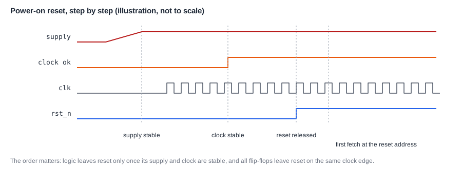
First the supply voltage rises and settles; a power-on reset circuit holds reset active meanwhile. Then the oscillator starts and the PLL locks. Only when supply and clocks are stable is reset released, and the processor fetches its first instruction from the reset address. Many SoCs release reset in stages: clocks and memories first, then the boot processor, and the other blocks later, under the control of the boot software.
Power-on is not the only reset. A watchdog timer resets the chip if software stops responding; software can request a reset; a debugger can reset the processor. Each kind may reset a different part of the chip, and each must leave the system in a consistent state.
Asynchronous Assertion, Synchronous Release
Reset can be asserted, switched on, at any moment, because it simply forces flip-flops to their reset values. Its release is different. If reset ends close to a clock edge, some flip-flops may see the end of reset in this cycle and others in the next, and a state machine could start with half its bits running, in a state that should be impossible. So reset is released synchronously: a reset synchronizer, built like the two-flip-flop synchronizer above, makes the release happen in step with the clock of each domain, and every flip-flop in the domain leaves reset in the same cycle.
A typical small design uses exactly this style: its flip-flops reset as soon as the active-low reset input rst_n goes to 0, and reset is held for a few clock cycles and released right after a rising edge, so all of them start together.
Where Does This Matter?
Reset bugs are among the hardest to find, because simulation usually starts from one clean reset and hides them. Chips that fail only on some power-ups, or after a watchdog reset but not after a power-on reset, usually have a block whose reset order, reset release or reset value was wrong. Verification teams therefore run dedicated reset tests, including resets in the middle of traffic.
Reset Values Decide the First Cycle
Choosing what each register resets to is part of the design. A simple timer shows why. It has a 64-bit counter mtime and a 64-bit compare value cmp, and raises its interrupt request timer_irq whenever mtime is greater than or equal to cmp:
| Register | Reset value | Why |
|---|---|---|
| mtime | 0 | time starts at zero at reset, so software can measure from boot |
| cmp | 0xFFFF_FFFF_FFFF_FFFF | the largest value, so the interrupt cannot fire until software sets a deadline |
If cmp reset to 0, the comparison mtime >= cmp would be true from the very first cycle, and the timer would request an interrupt before any software had set up a handler for it. The width matters too: at 100 MHz a 64-bit counter wraps around after about 5,800 years, while a 32-bit counter would wrap after 43 seconds.
The UART makes the same kind of choice. Its DIV register, the number of clock cycles per bit, resets to 16, a rate that works. Boot code can print messages before it has configured anything, and the output is readable.
Quick Check
Q: Suppose a UART's DIV register reset to 0. What would go wrong if software wrote TXDATA before setting DIV?
Show Answer
With 0 clock cycles per bit, the UART cannot send a valid bit; depending on the design it sends garbage or never finishes a byte. Resetting DIV to a working rate makes early output from boot code readable without any setup.
From Reset to the First Output
Take a small SoC in simulation, with no boot ROM. The program is placed directly in a 64 KB TCM at address 0, the way a debugger can load code into a chip's memory through its debug port, and then reset is released. A trace of the instruction in the core's execute stage on every cycle shows what happens next for a small program that prints text:
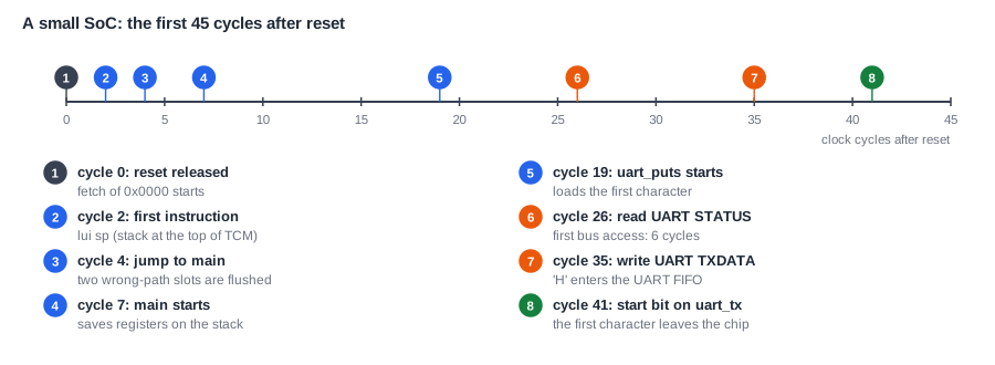
| Cycle after reset | Event |
|---|---|
| 2 | the first instruction, at address 0, executes; cycles 0 and 1 fetched and decoded it |
| 4 | the call to main executes; the two instructions fetched after it are discarded |
| 7 | main starts, saving registers on the stack in the 1-cycle TCM |
| 19 | main calls the string printer |
| 26 | the first access that leaves the CPU subsystem: a read of the UART STATUS register, 6 cycles over the bus |
| 35 | the first character is written to the UART's TXDATA register |
| 41 | the UART drives the start bit of that character onto its uart_tx pin |
At a 100 MHz clock, the chip shows its first sign of life 410 ns after reset. In a real product, much more happens before that point: the supply ramps, the PLL locks, and a boot ROM checks and loads the firmware, which can take milliseconds. Each of those steps is designed, and verified, as part of the system.
Reset Domains
Just as a chip has several clock domains, it has several reset domains: groups of flip-flops that are reset together. A watchdog reset may restart the processors but keep the always-on block that counts time; a software reset may restart one peripheral while the rest keeps running; the debug logic usually has its own reset, so that a debugger stays connected while the chip it is examining restarts.
Signals between reset domains need care too. If a block is reset while it is in the middle of a bus transaction, its partner may wait forever for a response that will never come, or receive a response for a request it never made. Designers therefore make sure a block is idle, its transactions drained, before it is reset alone, and they check every signal that crosses from one reset domain to another, the same way they check clock-domain crossings. A very small SoC may have a single reset domain, but a real SoC's reset architecture is planned in the spec alongside its clocks.
Common Mistakes
Mistake #1: Releasing reset asynchronously
If reset ends at an arbitrary moment, flip-flops near a clock edge may leave reset in different cycles. Assert reset at any time, but release it synchronously to the clock of each domain.
Mistake #2: Passing signals between domains directly
A wire from one clock domain into flip-flops of another is a metastability hazard, and simulation rarely shows it, because simulated signals never become metastable. Every crossing needs a synchronizer, a handshake or an asynchronous FIFO, and CDC checking tools to confirm it.
Mistake #3: Choosing reset values without thinking about the first cycle
A reset value that enables an interrupt, starts a transfer or selects an invalid mode acts before software can intervene. Reset values should leave each block idle and safe.
Practice Exercise
Challenge: Counters, Wraps and Boot Time
(a) A timer counts every cycle at 100 MHz. How long do a 32-bit and a 64-bit counter take to wrap around, and which width does a system that must run for years without reboot need? (b) A real chip's PLL needs 50 microseconds to lock after the oscillator starts, and its boot ROM then takes 200,000 cycles at 100 MHz to load and check the firmware. How long after the PLL starts does the firmware's first instruction run, ignoring the supply ramp? (c) Compare that with the 41 cycles from reset to the first output in the small SoC above.
Hint
An n-bit counter wraps after 2n counts; each count is 10 ns. 200,000 cycles at 10 ns each is 2 ms.
Solution
(a) 32 bits: 232 x 10 ns = 42.9 seconds. 64 bits: 264 x 10 ns = 1.84 x 10¹¹ seconds, about 5,845 years. A system that runs for years needs the 64-bit counter, or software that handles the wrap every 43 seconds, which is a common source of bugs. (b) 50 microseconds + 2,000 microseconds = 2.05 ms. (c) 41 cycles are 0.41 microseconds, about 5,000 times shorter: the simulation skips the PLL and the boot ROM, because it supplies a stable clock and preloads the program.
Summary
- Clocks come from an oscillator and PLLs and reach the flip-flops through a clock tree; each clock defines a clock domain, and SoCs have many.
- Signals crossing domains can go metastable: single bits need synchronizers, multi-bit values need handshakes or asynchronous FIFOs.
- Reset is held until supplies and clocks are stable, asserted at any time and released synchronously, often in stages.
- Reset values decide the first cycle: a timer starts at 0 with its compare at the maximum, and a UART at a working rate.
- In simulation, with the program preloaded, a small SoC can run its first instruction a couple of cycles after reset and drive a UART start bit a few dozen cycles later.
