
A CPU subsystem is the processor core together with everything it needs close by: fast local memory, the logic that sends each access to the right place, the bus port to the rest of the chip, interrupt inputs and a debug connection. Integrating it well matters, because nearly everything the chip does starts with an instruction, and every cycle the core waits for memory or the bus is lost. This article explains the parts of a CPU subsystem, how an access is routed, what the bus port decides about performance, how interrupts and debug are connected, and what goes wrong at these boundaries.
11 min read | Beginner to Intermediate
What You'll Learn
- Name the parts of a CPU subsystem and what each does
- Explain how an address decides between local memory and the bus
- Estimate how the bus port's latency and outstanding transactions affect the core
- Describe how interrupts, debug and reset connect to the core
What a CPU Subsystem Is
A processor core on its own is a pipeline with an instruction port and a data port, as The Datapath explains. To be useful in an SoC, it needs more around it. Vendors usually deliver cores as a complete subsystem, sometimes called a core complex or a CPU cluster, with these parts already connected:
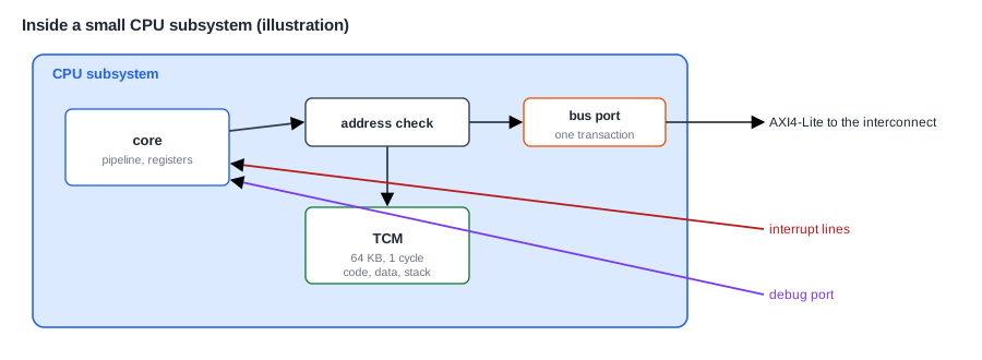
- The core itself.
- Local memory: a tightly coupled memory (TCM), caches, or both.
- An address decoder that sends each access to the local memory or out to the bus.
- A bus port, or manager port, that speaks the chip's interconnect protocol.
- Interrupt inputs, and often a small local interrupt controller and timer.
- A debug module, reached through JTAG or a similar port.
- Clock and reset inputs, and sometimes power control.
Routing Each Access
Every load, store and instruction fetch carries an address. A small decoder inside the subsystem looks at the high bits. If the address falls in the TCM range, the access goes to the TCM, which answers in one cycle. Otherwise it leaves the subsystem through the bus port and crosses the interconnect, as Memory Maps and Address Decoding explains.
In one small example SoC, a TCM access costs 1 cycle, an access to the on-chip SRAM across the bus costs 4, and an access to a peripheral behind a slower bus bridge costs 6. Those differences show up directly in run time. A test program that copied a buffer ran about 22 percent slower when the destination was in the SRAM rather than the TCM, with almost the same instructions.
This is why the first integration decision is what goes where. Code, the stack and data used in tight loops belong in the TCM or behind a cache. Large buffers and data shared with other blocks go further out. The linker script, described in Assembling, Linking and Loading, puts that decision into effect.
Instruction and Data Paths
A pipelined core fetches an instruction and accesses data in the same cycle, so the local memory needs two ports, or the two paths need separate memories. If both paths had to share one single-port memory, every load or store would stall a fetch. A TCM with one read-write port for data and one read port for instructions is a common answer, and Memories in a System describes that organization.
Quick Check
Q: A program keeps its stack in on-chip SRAM, which costs 4 cycles per access, rather than in the 1-cycle TCM. A function makes 2,000 stack accesses. How many extra cycles does that cost?
Show Answer
2,000 x (4 - 1) = 6,000 extra cycles, on a simple core that waits for every access. Moving the stack to the TCM is a one-line change in the linker script.
The Bus Port
The bus port decides how well the core can use the rest of the chip. Two properties matter most.
The first is latency: how many cycles a request takes to come back. Each stage of the interconnect, each clock crossing and each bridge adds to it. A simple in-order core waits for every load, so its CPI rises with each cycle of latency.
The second is how many transactions can be outstanding, that is, in flight at once. A simple port waits for each response before sending the next request. In one small SoC with such a port, a test program spent over a third of its run time with the core waiting on the bus. A port that allows several outstanding transactions can overlap them, but only if the core can issue another request while one is pending. A simple in-order core usually can't, which is one reason large cores have non-blocking caches. Outstanding Transactions and Bursts works through the numbers.
The protocol matters too. A simple protocol such as AXI4-Lite, or APB for peripherals, carries one word per transaction. A full protocol such as AXI carries bursts, so a cache line can be filled with one request. A core with caches needs a port that supports bursts, or every line fill turns into many slow single transfers.
Caches or TCM?
A small embedded core often has a TCM and no caches: its timing is fully predictable, and it is cheaper. A larger core uses caches to reach external memory, and may also have a TCM for code that must run with known timing, such as an interrupt handler. If a subsystem has caches, they create work at integration: DMA buffers must be handled carefully, as DMA Engines explains, unless the interconnect keeps the caches coherent.
Interrupts
A core has a small number of interrupt inputs. In RISC-V, a core has a machine external interrupt, a timer interrupt and a software interrupt, as Interrupts and Interrupt Latency describes. An SoC with dozens of interrupt sources combines them in an interrupt controller, which drives the core's external interrupt line. Interrupt Controllers explains that block.
Interrupt lines often cross clock domains, because devices may run on their own clocks. Each must be synchronized into the core's clock domain, as Clock Architecture and Clock Domain Crossings describes. The integrator also decides whether each line is level-sensitive or edge-triggered, which must match what the device and the controller expect.
Debug
A chip that can't be debugged can't be brought up. Most cores include a debug module that can halt the core, read and write registers and memory, set breakpoints and single-step. RISC-V defines a standard debug specification, so one debugger works with many cores. The debug module is usually reached through a JTAG port at the pins, or a two-wire variant, and in larger chips through a debug network that reaches every core.
Debug has security implications. A debugger can read anything, so production chips often lock the debug port, or require a key to unlock it. That must be decided at integration, as Security Architecture discusses.
Where Does This Matter?
Many SoC performance problems are found at this boundary. A core vendor quotes a benchmark score with fast memory, the SoC places the code in slow flash behind a long bus, and the real product runs at a fraction of that speed. A real bug from one small SoC shows another risk: a core that passed all its own tests with one-cycle memory lost a value while the pipeline waited for a slower bus, and computed wrong results in the system. The SoC team and flow article tells that story.
Reset and Boot
At reset, the core starts fetching from a fixed reset vector. The integrator decides what is there: a boot ROM, the start of flash, or a TCM loaded by other means. Some cores take the reset vector as an input pin, set by the SoC, which makes this choice a wiring decision. Boot ROM and the Boot Flow covers the rest. Reset must also be released in the right order: the memories and bus the core needs must be out of reset before the core makes its first fetch.
Configuration Choices
A licensed core usually comes with many options to set at integration time. Typical ones include:
- which instruction set extensions to include, such as multiply, floating point or compressed instructions;
- TCM and cache sizes;
- the number of interrupt lines and priority levels;
- debug features, such as the number of hardware breakpoints and trace;
- the bus protocol, width and number of outstanding transactions;
- whether there is a memory protection unit or an MMU.
Each one affects area and power, and some affect software. Compiling software for an extension the core lacks makes it fail, as What an ISA Defines explains. So the configuration is recorded in the spec, and the software build is set up to match.
Quick Check
Q: A core runs at 200 MHz with a CPI of 1.3 when all its data is in the TCM. Thirty percent of its instructions are loads or stores. If all its data moves across a bus costing 6 cycles per access, what is its CPI, assuming the core waits for each access?
Show Answer
Each data access costs 5 extra cycles: 0.3 x 5 = 1.5 extra cycles per instruction, so the CPI becomes 2.8, more than twice as slow.
More Than One Core
Many SoCs have several CPU subsystems, each with a different job: a large application cluster, a small real-time core for control, a tiny core in the always-on domain to manage power. Each is integrated the same way, but they must also cooperate. They need a way to send each other messages, usually a small hardware mailbox that raises an interrupt on the other side. They need agreed rules about which memory each may use. And at boot, one core usually starts first and releases the others. Multicore Integration and Coherent Interconnects covers cores that share data through caches.
Common Mistakes
Mistake #1: Putting hot code far from the core
Running time-critical code from slow memory throws away the core's performance. Place code, stack and frequently used data in local memory, or behind a cache.
Mistake #2: Testing the core only with ideal memory
A core tested with one-cycle memory may fail with a slower bus. Test the subsystem with realistic and random memory latencies.
Mistake #3: Forgetting to secure the debug port
An open debug port in a shipped product lets anyone read memory and secrets. Decide the debug policy as part of integration, and lock the port when it is needed.
Practice Exercise
Challenge: Where Should It Go?
A small SoC has 32 KB of TCM at 1 cycle and 256 KB of SRAM across the bus at 5 cycles. These numbers are assumptions for this exercise. The firmware has 20 KB of code, 4 KB of stack, a 2 KB table used in every loop, and a 200 KB image buffer filled by a camera through DMA. (a) What goes in the TCM? (b) What goes in the SRAM, and why? (c) If the table were placed in SRAM instead, and the main loop reads it 50,000 times per second, how many cycles per second would be lost, and what share is that of a core running at 100 MHz?
Hint
The TCM holds 32 KB. Data shared with DMA is usually best in memory the DMA engine can reach on the bus.
Solution
(a) The code, the stack and the table: 20 + 4 + 2 = 26 KB, which fits. (b) The image buffer, which is far too large for the TCM and is written by DMA over the bus. (c) 50,000 x (5 - 1) = 200,000 cycles per second, which is 0.2 percent of a 100 MHz core, small here, but it would grow if the loop ran faster.
Summary
- A CPU subsystem is the core plus local memory, an address decoder, a bus port, interrupts, debug, and clock and reset.
- The address decides whether an access stays local, in about one cycle, or crosses the bus, in several.
- Bus latency and the number of outstanding transactions set how much the core waits.
- Interrupts need synchronizing and the right sensitivity; debug needs a security policy.
- Configuration options change area, power and software, so they belong in the spec.
