
The system architecture spec is the document that defines an SoC before it is built: its blocks and how they connect, the memory map, the registers software sees, the clocks, resets, interrupts and power domains, the error behavior, and the performance each part must reach. Every team works from it, so an error in the spec becomes an error in the chip, often in several places at once. This article explains what a spec contains and who reads each part, how specs are written, reviewed and kept consistent, walks through the spec of a small SoC section by section, and shows how one vague word in a register description became a real bug.
13 min read | Beginner to Intermediate
What You'll Learn
- List the sections of a system architecture spec and who uses each
- Explain how specs are kept precise and consistent, including generated outputs
- Read the main sections of a real SoC spec: blocks, memory, registers, interrupts, clocks, resets, errors, budgets
- Write a precise specification entry for a new block
One Document, Many Readers
Requirements say what the product needs; the system architecture spec says what the chip will be, in enough detail that each team can build its part without asking. It is the answer to the requirements, described in From Use Cases to Requirements, and the input to every later phase of the flow in The SoC Team and Flow.
Because so many people read it, a spec is organized by topic, and most specs, whatever the company, contain the same sections:
| Section | What it defines | Main readers |
|---|---|---|
| block diagram and block list | every block, its version or source, and the buses between them | everyone |
| memory map | which block owns which address range | integration, software, verification |
| register maps | every software-visible register, its fields, access type and reset value | software, verification, IP teams |
| interrupt map | which source drives which interrupt line, and its type | software, integration |
| clocks, resets and power | clock sources and frequencies, reset sequence and domains, power domains and modes | integration, implementation |
| performance and power budgets | bandwidth, latency and power per use case | architects, implementation, performance modeling |
| error handling | responses to illegal accesses, timeouts, memory errors | software, verification |
| debug, test and security | debug access, scan and memory test, secure boot and key storage | DFT, validation, security |
The spec describes what each part must do, not how it is built inside. It states that the UART has an 8-byte transmit FIFO and what its status bits mean; it does not prescribe the UART's internal state machine. That leaves the IP team free to design the block, and makes the spec the reference against which verification checks it.
Keeping the Spec Precise
A spec is only useful if every reader understands it the same way. Three practices make that possible.
Precise Wording
Every number has a unit, every register field its exact bits, access type and reset value, and every behavior its edge cases: what a write-only register returns when read, what happens when a FIFO is full and software writes anyway, which events a status bit includes. Words like "busy", "ready" or "done" are defined, not assumed. Many companies also use requirement-style wording: "shall" for what is mandatory, "may" for what is optional.
One Source, Generated Outputs
The parts of a spec that become code, the memory map and the register maps above all, are not typed separately into the documentation, the RTL and the software. They are written once in a machine-readable description and generated into everything that needs them:
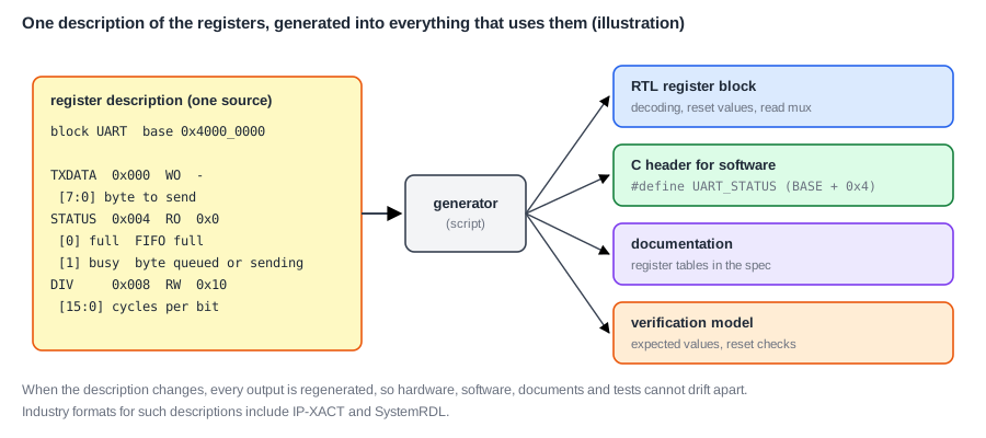
When an address or a field changes, every output is regenerated, so the chip, its drivers, its documents and its tests cannot drift apart. Industry formats for such descriptions include IP-XACT and SystemRDL, and many companies use their own spreadsheets or scripts. Memory-Mapped I/O and Registers shows how software uses the generated registers.
Versions and Change Control
A spec changes during a project, and every change affects several teams. Specs are therefore versioned, every change is reviewed by the teams it affects, and after the spec freeze, changes need formal approval. A change log at the front records what changed, when and why. A team that implements an old version of the spec builds the wrong chip, however good its work is.
Quick Check
Q: The memory map is kept in a spreadsheet for the documentation, typed by hand into the interconnect RTL, and copied into a C header by the software team. What will happen over a long project?
Show Answer
The three copies will drift apart: an address changed in one is forgotten in another, and the chip, its software and its documentation disagree. Generating all three from one source prevents it.
A Small SoC's Spec, Section by Section
A small SoC with one core and a few peripherals can fit its whole spec on a few pages. Here are the main sections of one.
Block List
| Block | Function | Interfaces |
|---|---|---|
| CPU subsystem | RV32I core, 64 KB TCM, one-outstanding AXI4-Lite manager port | AXI4-Lite manager |
| interconnect | AXI4-Lite, 1 manager to 2 subordinates, DECERR for unowned addresses | AXI4-Lite |
| system SRAM | 16 KB, single port, byte strobes | AXI4-Lite subordinate |
| APB bridge | AXI4-Lite to APB, up to 16 peripherals in 4 KB slots, SLVERR for empty slots | AXI4-Lite subordinate, APB manager |
| UART | transmit only, 8N1, 8-byte FIFO, programmable bit time | APB, pin uart_tx |
| timer | 64-bit cycle counter and compare value, interrupt output | APB, pin timer_irq |
| GPIO | 32 outputs, 32 inputs | APB, pins gpio_out, gpio_in |
| simulation control | ends a simulation with a result code (simulation only) | APB |
Memory Map
The TCM is at 0x0000_0000 (64 KB), the system SRAM at 0x2000_0000 (16 KB), and the peripheral window at 0x4000_0000 (64 KB), with the UART in slot 0, the timer in slot 1, the GPIO in slot 2 and simulation control in slot F. Everything else is unowned. Memory Maps and Address Decoding explains how the map is chosen and decoded.
Register Maps
For each peripheral, the spec lists every register. This is the UART's:
| Offset | Name | Access | Reset | Description |
|---|---|---|---|---|
| 0x000 | TXDATA | write only | - | bits 7:0: byte to send, queued in the FIFO; ignored when the FIFO is full; reads as 0 |
| 0x004 | STATUS | read only | 0x0 | bit 0: FIFO full; bit 1: busy, meaning a byte is queued or being sent |
| 0x008 | DIV | read/write | 0x10 | bits 15:0: clock cycles per bit |
Every word in this table becomes code. The driver polls bit 0 of STATUS before writing a byte, a test checks the reset value of DIV, and the integration team gives the UART the slot at 0x4000_0000. The definition of busy was not always this precise. In the first version of this SoC, the spec said only "busy", and the UART reported busy only while a byte was on the wire, not while bytes were waiting in the FIFO. A program that waited for the UART to finish before ending stopped too early and lost its last characters. The fix was in the RTL, but the real fix was the definition: "a byte is queued or being sent".
Interrupt Map
The timer drives the interrupt line timer_irq, level-sensitive and active high: it stays high while the counter is greater than or equal to the compare value, until software moves the compare value. In this small SoC the line just goes to a pin; a larger SoC's interrupt map lists hundreds of sources, each with its number, type (level or edge) and destination.
Clocks and Resets
One clock, nominally 100 MHz, drives every block; there are no clock-domain crossings. One active-low reset, rst_n, resets every block, asserted asynchronously and released in step with the clock. The reset values that matter are part of the register maps: UART DIV resets to 16, the timer counter to 0 and its compare value to the maximum 64-bit value, so that no interrupt fires before software sets one up. Clocks and Resets in a System explains why.
Error Handling
Every access gets an answer. An address that no interconnect subordinate owns gets a decode error (DECERR) from the interconnect; an address in the peripheral window whose slot is empty gets a slave error (SLVERR) from the bridge. Reads that fail return 0; the CPU subsystem records the error and the core continues. A test can check this rule by reading unowned addresses, as Buses and Transactions shows.
Performance
The spec states the latency of each path as seen by the core: 1 cycle for the TCM, 4 cycles for the system SRAM, 6 cycles for a peripheral, with one transaction outstanding at a time. These numbers are checked in simulation, and they are the basis for every bandwidth estimate in Latency and Bandwidth.
Where Does This Matter?
Real SoC specs run to hundreds or thousands of pages, split into a top-level system spec and separate specs per subsystem and per block. They are reviewed formally, with each affected team signing off, and they are the reference for customers too: a chip's public datasheet and reference manual are largely derived from its internal spec, register maps included.
Quick Check
Q: Software writes 0x4 to the UART's DIV register. Using the spec, what is the full address of the write, and what does it change?
Show Answer
The UART is in slot 0 at 0x4000_0000 and DIV is at offset 0x008, so the address is 0x4000_0008. It sets 4 clock cycles per bit, making the UART four times faster than its reset value of 16.
What Makes a Spec Entry Good
A useful test for every entry: could two engineers who never talk to each other, one building the block and one writing its driver, produce parts that work together from the entry alone? That requires answering, for each register:
- Where is it? Offset, width, which bits are used, and what reads of unused bits return.
- Who may change it? Access type: read/write, read only, write only, write 1 to clear.
- What is it at the start? Reset value, and which reset domain resets it.
- What does each field mean, including its edge cases? What happens on writes when the block is busy, on illegal values, on reads with side effects.
- What does the block do by itself? Interrupts it raises, status bits it changes, and when.
The "busy" story above failed the last point: the meaning of a status bit, as the hardware changes it, was not stated precisely. Most register-level integration bugs are of this kind.
The Spec After Tape-Out
The spec does not end with tape-out. During bring-up, the validation team tests the silicon against it, and every difference is either a bug in the chip or a mistake in the spec. Differences that cannot be fixed in hardware are published as errata: a list of known deviations from the documented behavior, each with a description and, where possible, a software workaround. A typical erratum reads like a spec entry corrected after the fact, for example "the busy bit may clear one cycle early; software must wait one extra cycle".
The customer-facing documents, the datasheet and the reference manual, are derived from the internal spec, with its register maps nearly unchanged. And the spec becomes the starting point of the next chip: the next version keeps the memory map and register layout of the blocks it reuses, so that existing drivers keep working, which is why decisions made in the first spec, such as where each block lives and how its registers are arranged, can last for many product generations.
Common Mistakes
Mistake #1: Leaving behavior implicit
If the spec does not say what a status bit includes, what a write-only register reads as, or what happens on an unowned address, each team guesses, and the guesses differ. Write the edge cases down.
Mistake #2: Keeping several hand-edited copies
When the RTL, the C headers and the documents are edited separately, they drift apart. Generate them from one source, and review changes to that source like code.
Mistake #3: Specifying the inside of blocks
A spec that prescribes internal implementation details constrains the IP team without helping anyone else, and becomes wrong as soon as the design improves. Specify interfaces and behavior; leave the internals to the block's own design document.
Practice Exercise
Challenge: Specify a New Peripheral
The next version of this SoC adds a PWM (pulse-width modulation) block that drives one output pin high for DUTY clock cycles out of every PERIOD cycles, and can be switched on and off. (a) Choose its slot and base address. (b) Write its register map entries: offset, name, access, reset value and description. (c) Name two edge cases your entries must state, and how you define them.
Hint
Slots 0, 1, 2 and F are taken. Think about what the pin does after reset, and what happens if DUTY is larger than PERIOD.
Solution
(a) Slot 3, base 0x4000_3000. (b) One possible map: 0x000 CTRL, read/write, reset 0x0, bit 0 EN (1 = running, 0 = pin held low); 0x004 PERIOD, read/write, reset 0x0, bits 31:0 cycles per period; 0x008 DUTY, read/write, reset 0x0, bits 31:0 high cycles per period. Unused bits of CTRL read as 0 and ignore writes. (c) Examples: the pin is low after reset and whenever EN = 0, so nothing moves before software configures the block; if DUTY >= PERIOD the pin stays high, and if PERIOD = 0 the pin stays low; new PERIOD and DUTY values take effect at the start of the next period, so a change never produces a glitch. Any precise definition works, as long as it is written down.
Summary
- The system spec defines blocks, connections, memory map, registers, interrupts, clocks, resets, power, budgets, errors, debug and security, for many readers at once.
- It specifies interfaces and behavior, not block internals, with every unit, field, reset value and edge case stated.
- Memory and register maps are generated from one machine-readable source into RTL, C headers, documents and tests.
- A small SoC's spec fits on a few pages: eight blocks, three address regions, one clock, one reset, one interrupt, two error responses and three path latencies.
- A vague "busy" bit in the UART's register map caused a real bug; most register-level integration bugs come from undefined behavior.
