
Inside a processor, the hardware that carries out instructions has two halves. The datapath holds and moves the data: the program counter, the memories, the register file, the ALU and the switches between them. The control decides, for each instruction, which of those paths are used. This article explains each block of the datapath, what a multiplexer does and why there are so many, how control signals make one set of hardware run every instruction, and follows three real instructions of a RISC-V program through it, one control signal at a time.
13 min read | Beginner
What You'll Learn
- Name the blocks of a processor datapath and explain what each one does
- Explain how multiplexers and control signals steer values between blocks
- Trace an arithmetic, load, store and branch instruction through the datapath
- List the operations of a RISC-V ALU and explain what happens to the rest
Datapath and Control
The datapath is every piece of hardware that stores, moves or transforms the values a program works on. The control is the logic that looks at the current instruction and sets the switches of the datapath so that this instruction, and not another, gets done. A useful way to think of it: the datapath is the set of roads, and the control sets the traffic lights at every junction, once per instruction.
This split is the key to how a processor can run dozens of different instructions without dozens of separate circuits. An addition, a load and a branch all use the same adder, the same register file and the same wires; only the control settings differ.
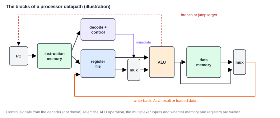
The Blocks, One by One
The picture above shows the datapath in the order an instruction passes through it, matching the five steps of The Instruction Cycle.
Program Counter and Instruction Memory
The program counter (PC) is a 32-bit register holding the address of the current instruction. It feeds the instruction memory, which returns the 32-bit instruction stored at that address. In many small processors the instruction memory and the data memory are separate ports onto one shared memory, so fetching an instruction and loading data can happen in the same cycle.
Decoder
The decoder takes the instruction apart. RISC-V places each field at a fixed position in the 32 bits: the opcode, which says what kind of instruction it is, in bits 6 to 0; the destination register rd in bits 11 to 7; a small operation code, funct3, in bits 14 to 12; the source registers rs1 and rs2 in bits 19 to 15 and 24 to 20. The decoder also assembles the immediate, the constant built into the instruction, whose bits are spread over the instruction differently in each of the five formats, and sign-extends it to 32 bits. RISC-V Instruction Formats and Encoding shows each format bit by bit.
From the opcode and funct3, the decoder produces the control signals. In a simple processor the decoder is a single block of combinational logic. Its outputs are the three register numbers, the immediate, and a dozen or so control signals described below.
Register File
The register file holds the 32 general-purpose registers. It has two read ports, which deliver the values of rs1 and rs2 in the same cycle, and one write port, which stores a result into rd at the clock edge when the write is enabled. Registers and the Register File shows how it is built.
ALU
The ALU, arithmetic logic unit, takes two 32-bit operands, A and B, and a 4-bit operation code, and produces a 32-bit result. RV32I needs only ten operations:
| Operation | Result | Used by |
|---|---|---|
| ADD, SUB | A + B, A - B | add, addi, sub, every load and store address, lui and auipc |
| AND, OR, XOR | bitwise logic | and, or, xor and their immediate forms |
| SLL, SRL, SRA | shift A left, logical right, arithmetic right by B[4:0] | sll, srl, sra and their immediate forms |
| SLT, SLTU | 1 if A < B (signed / unsigned), else 0 | slt, sltu and their immediate forms |
The shift amount is only the low 5 bits of B, because shifting a 32-bit value by more than 31 places makes no sense. Numbers in Hardware explains signed and unsigned comparison and the two right shifts. Comparators and ALUs shows how an ALU is built from gates.
Branch Comparator and Target Adder
A branch must compare two registers and, if the condition holds, jump to PC + offset. Some textbook designs use the ALU to subtract and test the result. Many real cores have a separate comparator that checks the six branch conditions (equal, not equal, less than and greater or equal, signed and unsigned) and a separate adder for the target address instead. The ALU stays free, and the branch decision is ready at the same time as everything else in the execute step.
Data Memory
The data memory serves loads and stores. Its address comes from the ALU (register + offset), the data to store comes from the rs2 register, and for byte and halfword accesses extra logic selects or places the right bytes within the 32-bit word, as described in Memory, Addresses and Endianness.
Multiplexers: the Switches
Wherever two or more values could go into the same input, the datapath has a multiplexer (mux): a circuit with several data inputs, one output and a select signal that decides which input passes through. A 2-to-1 mux with select 0 passes its first input, with select 1 its second. Digital Multiplexer Circuit shows how one is built.
A simple RV32I processor has four important muxes:
| Mux | Inputs | Why |
|---|---|---|
| ALU operand A | rs1 value, PC, zero | most instructions use rs1; auipc adds to the PC; lui adds to zero |
| ALU operand B | rs2 value, immediate | add uses a register, addi and loads use the constant from the instruction |
| Write-back value | ALU result, loaded data, PC + 4 | arithmetic writes its result, loads write memory data, jumps write the return address |
| Next PC | PC + 4, branch or jump target | sequential code or a taken branch or jump |
The select inputs of these muxes, together with the ALU operation and the enables for register and memory writes, are exactly the control signals the decoder produces.
Quick Check
Q: Which ALU operation does the load lw a5, 8(a4) use, and which inputs do the operand muxes select?
Show Answer
ADD. Operand A selects the rs1 value (register a4), operand B selects the immediate (8). The sum is the memory address. Loads and stores use the ALU as an address adder.
Control Signals
These are the control signals a simple decoder sets for each kind of instruction. "A" and "B" are the operand mux selects, "imm" means the immediate:
| Instruction kind | A | B | ALU op | reg_write | mem_read | mem_write | PC change |
|---|---|---|---|---|---|---|---|
| register-register (add, sub, ...) | rs1 | rs2 | from funct3 and bit 30 | 1 | 0 | 0 | - |
| register-immediate (addi, andi, ...) | rs1 | imm | from funct3 | 1 | 0 | 0 | - |
| load (lw, lbu, ...) | rs1 | imm | ADD | 1 | 1 | 0 | - |
| store (sw, sb, ...) | rs1 | imm | ADD | 0 | 0 | 1 | - |
| branch (beq, bne, ...) | - | - | - | 0 | 0 | 0 | if condition true |
| lui | zero | imm | ADD | 1 | 0 | 0 | - |
| auipc | PC | imm | ADD | 1 | 0 | 0 | - |
| jal / jalr | - | - | - | 1 (PC + 4) | 0 | 0 | always |
The write enables matter most. A store has no destination register: bits 11 to 7, where rd would be, hold part of the store's offset instead. If reg_write were 1 for stores, the processor would write some value into whichever register those bits happen to name. Likewise mem_write must be 0 for everything except stores, or every instruction would scribble over memory. The unused mux selects, marked "-", can be anything, because nothing uses their result.
A few more signals, which do not appear in the table, tell the comparator which branch condition to test (the funct3 field), say whether the instruction is a branch, jal or jalr, and tell the hazard logic which source registers the instruction really reads. That is twelve control signals in all.
Three Instructions Through the Datapath
Consider a program that writes characters to a console device at address 0xF000_0004. The compiler produced these three instructions to set up the address and send the first character, the letter 'H' (0x48), which it had already placed in a5 with an earlier li a5, 72:
  18:  f00005b7   lui   a1,0xf0000     # a1 = 0xF000_0000
  30:  00458593   addi  a1,a1,4        # a1 = 0xF000_0004
  3c:  00f5a023   sw    a5,0(a1)       # console = a5
lui a1, 0xf0000. The decoder sees the LUI opcode and builds the immediate 0xF000_0000 (the 20-bit constant placed in the upper bits). It sets operand A to zero, operand B to the immediate, the ALU to ADD and reg_write to 1. The ALU computes 0 + 0xF000_0000, the write-back mux selects the ALU result, and a1 receives 0xF000_0000. Using the adder with a zero input avoids a separate path just for lui.
addi a1, a1, 4. Now operand A selects rs1, the value of a1, and operand B the immediate 4. The ALU adds them, and a1 becomes 0xF000_0004. The data memory sees mem_read and mem_write both 0 and does nothing.
sw a5, 0(a1). The register file reads both a1 (rs1) and a5 (rs2). Operand A is a1, operand B the immediate 0, and the ALU computes the address 0xF000_0004. The data memory port receives that address, the value of a5 as data and mem_write = 1. reg_write is 0, so no register changes. Because the memory map assigns that address to the console, the 'H' appears on the console.
The same adder did three different jobs: building a constant, computing a value and computing an address. Only the control signals changed.
No Multiplier: What Happens to a * b
The ALU has no multiply. RV32I leaves multiplication and division to an optional extension called M, so that the smallest cores do not have to pay for a multiplier. A core without it can still run C code that multiplies: the compiler calls a small library routine, __mulsi3, that multiplies with shifts and additions, the way multiplication is done on paper in binary:
00000198 <__mulsi3>:            # a0 = a0 * a1
 198:  mv    a2,a0              # a2 = multiplicand
 19c:  li    a0,0               # a0 = result = 0
 1a0:  andi  a3,a1,1            # loop: lowest bit of the multiplier
 1a4:  beqz  a3,1ac             #   if it is 1,
 1a8:  add   a0,a0,a2           #     add the multiplicand to the result
 1ac:  srli  a1,a1,0x1          #   next multiplier bit
 1b0:  slli  a2,a2,0x1          #   multiplicand x 2
 1b4:  bnez  a1,1a0             #   repeat while bits remain
 1b8:  ret
One multiplication costs several instructions per bit of the multiplier, plus the call and return. Multiplying two 12 x 12 matrices takes 12 x 12 x 12 = 1,728 multiplications. Each is one call into __mulsi3 and one return, so the program executes 2 x 1,728 = 3,456 jumps for them, and in one test those were almost all the jumps in the program. With the M extension, each of those calls would become a single mul instruction.
Where Is This Used?
This datapath, with these blocks, is at the heart of every RISC processor, from tiny microcontrollers to large server cores. Bigger cores replicate the blocks, with several ALUs, a multiplier and more register-file ports, and add more stages, but the roles stay the same. Choosing which extensions to include, such as M for multiply, is one of the first decisions when a team configures a RISC-V core for a product.
Quick Check
Q: For auipc ra, 0x0 at address 0x04, which inputs do the operand muxes select, and what does ra receive?
Show Answer
Operand A selects the PC (0x04), operand B the immediate (0x0 shifted into the upper bits, so 0). The ALU adds them, and ra receives 0x0000_0004.
Common Mistakes
Mistake #1: Thinking each instruction has its own hardware
All instructions share the same blocks; control signals reconfigure the paths for each one. Adding an instruction usually means adding a decoder case and perhaps a mux input, not a new datapath.
Mistake #2: Leaving a write enable on
A stray reg_write or mem_write is one of the most common processor bugs. It silently corrupts a register or memory location that a later instruction reads, so the failure shows up far from its cause.
Mistake #3: Mixing up the signed and unsigned variants
SLT and SLTU, and SRA and SRL, differ only in how they treat the top bit. Mixing them up gives correct results for small positive numbers and wrong ones for everything else, which makes the bug easy to miss in testing.
Practice Exercise
Challenge: Set the Control Signals
For each instruction, give operand A, operand B, the ALU operation, reg_write, mem_read and mem_write, and say what the write-back mux selects: (a) lbu a5, 0(a4); (b) sub a0, a1, a2; (c) bnez a5, 3c. Then answer: (d) Assume a program executes 72,000 instructions, of which 1,000 are loads, 1,000 stores and 10,000 branches. How many of its instructions write a value through the data memory port?
Hint
Use the control-signal table. A branch uses the comparator, not the ALU. Only one kind of instruction writes memory.
Solution
(a) A = rs1 (a4), B = imm (0), ADD, reg_write 1, mem_read 1, mem_write 0; the write-back mux selects the loaded data (zero-extended byte). (b) A = rs1 (a1), B = rs2 (a2), SUB (funct3 000 with bit 30 set), reg_write 1, mem_read 0, mem_write 0; write-back selects the ALU result. (c) No ALU result is used; the comparator tests a5 != zero, and the target adder computes the address 0x3C. reg_write, mem_read and mem_write are all 0. (d) Only stores write memory: 1,000 of 72,000 instructions, about 1.4 percent.
Summary
- The datapath is the PC, instruction memory, decoder, register file, ALU, branch comparator, data memory and the muxes between them.
- Multiplexers choose ALU operands, the write-back value and the next PC; the decoder's control signals set them.
- Write enables decide which instructions change registers or memory; a wrong enable silently corrupts state.
- The RV32I ALU has ten operations; lui, auipc, loads and stores all reuse its adder.
- Without the M extension, multiplication is a shift-and-add routine reached by a call: multiplying two 12 x 12 matrices costs 3,456 jumps.
