
Almost every digital chip, from a microcontroller to a server processor, is driven by a clock: a signal that ticks at a fixed rate and tells every register when to take its next value. The clock turns the work of a processor into a count of cycles, and its rate decides how long each cycle lasts. This article explains what a clock is, how registers and logic share each cycle, what sets the fastest possible clock, and how a cycle count becomes time, using a 32-bit adder built from real gates as the example.
13 min read | Beginner
What You'll Learn
- Define clock period, frequency and clock edge, and convert between them
- Explain how registers and combinational logic share a clock cycle
- Calculate the shortest clock period of a path from its delays
- Convert a program's cycle count into run time at a given clock frequency
The Clock Signal
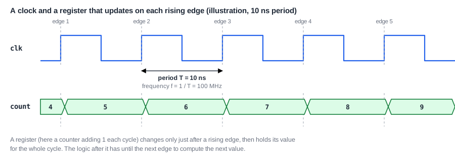
A clock is a signal that switches between 0 and 1 over and over at a fixed rate. Each moment where it rises from 0 to 1 is a rising edge, and the time from one rising edge to the next is the clock period, written T. The stretch of time between two rising edges is one clock cycle, so a cycle and a period are the same length of time.
The number of cycles per second is the clock frequency, f, measured in hertz (Hz). Frequency and period are each other's inverse: f = 1 / T. Chips run at millions or billions of cycles per second, so the usual units are megahertz (MHz, a million cycles per second) and gigahertz (GHz, a billion), with periods in nanoseconds (ns, a billionth of a second) and picoseconds (ps, a thousandth of a nanosecond):
| Frequency | Period | Typical of |
|---|---|---|
| 16 MHz | 62.5 ns | small 8-bit microcontrollers |
| 100 MHz | 10 ns | a common FPGA design clock |
| 1 GHz | 1 ns | phone and embedded application processors |
| 4 GHz | 0.25 ns = 250 ps | desktop processors at full speed |
The clock comes from a crystal oscillator on the circuit board, usually multiplied up on the chip by a circuit called a PLL (phase-locked loop), and is spread to every register through a network of wires and buffers, the clock tree. Its job is the same everywhere: to mark the moments at which the chip's state may change.
Registers Change Only on the Edge
A processor's state lives in registers: groups of flip-flops, each storing one bit. A flip-flop has a data input D, an output Q and a clock input. On each rising edge it copies D to Q; at all other times it ignores D and keeps Q steady. A 32-bit register is 32 flip-flops sharing one clock. D Flip-Flop Circuit shows how one is built from gates.
Between the registers sits combinational logic: gates such as AND, OR and XOR, and the larger blocks built from them, like adders and multiplexers. Combinational logic has no memory. Its output depends only on its current inputs, and it needs some time, its delay, to settle after an input changes.
A design where every register loads on the same clock edge is synchronous, and almost all processors are built this way. The rule makes the design easy to reason about: just after an edge, registers present new values; during the cycle the logic computes from them; at the next edge the registers capture the results. The counter in the picture above is the smallest example. Its register holds 5, an adder computes 5 + 1 = 6 during the cycle, and at the next edge the register loads 6.
A processor works the same way at a larger scale. Its program counter, its 32 registers and the registers between its pipeline stages can all load on the rising edge of one clock. Everything it does in a cycle happens in the logic between those registers.
Quick Check
Q: A processor runs at 250 MHz. What is its clock period, and how many cycles does it run in one microsecond?
Show Answer
T = 1 / 250 MHz = 4 ns. One microsecond is 1,000 ns, so it runs 1,000 / 4 = 250 cycles in that time. (A frequency in MHz is also the number of cycles per microsecond.)
What Happens Inside One Cycle
For a design to work, each result must be ready before the edge that captures it. Follow one value from the register that sends it, the launch register, to the register that receives it, the capture register. Three delays add up along the way:
- Clock to Q: after the rising edge, the launch flip-flop needs a short time before its new value appears at Q.
- Logic delay: the value passes through the gates of the combinational logic, each adding its own delay.
- Setup time: the capture flip-flop needs its D input to be stable for a short time before the next rising edge, or it may store the wrong value.
The sum of these three must fit in one clock period. The time left over is the slack. Positive slack means the path works with time to spare; negative slack means the result arrives too late and the chip computes wrong values at that frequency.
A Worked Example: a 32-bit Adder
Addition is the most common operation in a processor, so a 32-bit adder between two registers is a good example. The circuit below was written in SystemVerilog, turned into real gates from an open-source 130 nm standard cell library by a synthesis tool, and timed by a static timing analysis tool at a 10 ns (100 MHz) clock. A cell library is a chip maker's catalog of ready-made gates. A newer process would be many times faster, but the way the delays add up stays the same.
module add_stage #(parameter N = 32) (
    input  logic         clk,
    input  logic [N-1:0] a_in, b_in,
    output logic [N-1:0] s_out
);
    logic [N-1:0] a, b;
    always_ff @(posedge clk) begin
        a     <= a_in;
        b     <= b_in;
        s_out <= a + b;
    end
endmodule
Registers a and b launch the two operands on one edge; register s_out captures their sum on the next. The timing tool reports the slowest path through the adder:
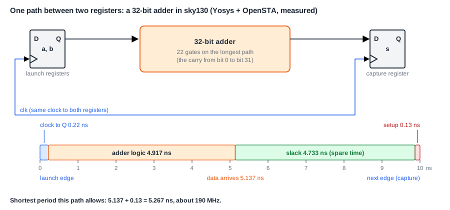
The longest path starts at bit 0 of an operand and ends at bit 31 of the sum. The reason is the carry: as in addition on paper, bit 31 of the sum depends on whether every lower bit pair produced a carry, so the carry signal must travel through the whole width. Here that path has 22 gates, and the numbers from the timing report are:
| Part of the path | Delay | Time |
|---|---|---|
| rising edge at the launch register | - | 0.000 ns |
| clock to Q of the launch flip-flop | 0.220 ns | 0.220 ns |
| 22 gates of the adder | 4.917 ns | 5.137 ns (data arrives) |
| next rising edge | - | 10.000 ns |
| setup time of the capture flip-flop | 0.130 ns | 9.870 ns (data required) |
| slack = required - arrival | 4.733 ns | met |
The result arrives at 5.137 ns and must be stable by 9.870 ns, so it makes it with 4.733 ns to spare. The clock could be faster. The shortest period this path allows is the arrival time plus the setup time, 5.137 + 0.130 = 5.267 ns, which is a frequency of 1 / 5.267 ns, about 190 MHz. At any period shorter than that, the slack turns negative.
The Critical Path Sets the Clock
A real chip has thousands or millions of register-to-register paths, and all of them share one clock. The slowest one, the path with the least slack, is the critical path, and it alone decides the highest clock frequency, often called Fmax. Making any other path faster does not help.
The width of the adder shows how strongly logic depth sets the clock. In the same test, going from 8 bits to 16 made the shortest period about 80 percent longer, and going from 16 bits to 32 made it about 40 percent longer again. The 32-bit adder needs about two and a half times the period of the 8-bit one.
A wider adder has a longer carry chain, so it needs a longer cycle. Doubling the width did not double the delay, because the synthesis tool built the upper part of the carry chain from compound gates that each cover more than one bit. Faster adder structures, which compute carries in parallel instead of one after another, are a classic way to shorten this path.
A whole processor does much more in a cycle than one addition. In a simple processor that finishes an instruction in a single cycle, one cycle must cover reading the instruction from memory, decoding it, reading registers, the ALU and a data memory access, one after another. That long critical path is the main reason processors are pipelined: registers placed in the middle of the work split it into shorter stages, so each cycle can be shorter. The 5-Stage Pipeline shows how a processor splits its work into five stages.
Where Does This Matter?
Timing closure, making every path meet the target clock, is one of the main tasks in chip design. Engineers run static timing analysis on every path after synthesis and after layout, then shorten failing paths by choosing faster gates, restructuring logic or adding pipeline registers. The process is covered in detail in Setup and Hold Checks.
From Cycles to Time
Processor simulations and performance counters count cycles, not seconds, because the cycle count depends only on the design and the program, while the time also depends on the clock. To turn cycles into time, multiply by the period, or divide by the frequency:
run time = cycles x clock period = cycles / clock frequency
Suppose a program that adds up 1,024 numbers takes 12,000 cycles on a simple processor. At 100 MHz that is 12,000 x 10 ns = 120,000 ns, or 120 microseconds. At 50 MHz the same program takes twice as long, 240 microseconds, although it executes exactly the same instructions in exactly the same number of cycles.
This separation is useful. A designer can change the processor's structure and compare cycle counts, change the clock and compare frequencies, and combine the two only at the end. The full relation, which also splits cycles into instructions and cycles per instruction, is the topic of The Performance Equation.
A Faster Clock Is Not Always Faster
The two factors often pull against each other. Splitting the work into more pipeline stages shortens the period, but it can also add cycles, for example when an instruction must wait for the result of the one before it. A design with a 20 percent faster clock that needs 30 percent more cycles for the same program is slower overall. Run time, not frequency, is what counts, which is why clock frequency alone is a poor way to compare processors.
Quick Check
Q: Design A runs a program in 10,000 cycles at 200 MHz. Design B runs it in 12,000 cycles at 250 MHz. Which finishes first?
Show Answer
A: 10,000 x 5 ns = 50 microseconds. B: 12,000 x 4 ns = 48 microseconds. B is faster despite needing 20 percent more cycles, because its clock is 25 percent faster.
One Clock or Many
A small processor often uses one clock. A full chip usually has several: the processor cores at one frequency, a memory interface at another, slow peripherals such as a UART at a third. The part of a design driven by one clock is a clock domain. Signals crossing from one domain to another need special circuits, because the receiving registers' edges do not line up with the sender's. Chips also slow or stop clocks to save power when there is no work. The SoC Design tutorial covers clock domains in a full system.
Common Mistakes
Mistake #1: Comparing processors by clock frequency alone
Run time is cycles multiplied by the period. A processor with a lower frequency that needs fewer cycles per program can be faster. Compare the time for the same program.
Mistake #2: Forgetting clock to Q and setup time
The logic delay is not the whole cycle. The flip-flop's clock-to-Q delay and the capture flip-flop's setup time come out of every period too: 0.35 ns of the 32-bit adder's budget in the example above.
Mistake #3: Mixing up the units
1 GHz is a 1 ns period, 100 MHz is 10 ns, 1 MHz is 1 microsecond. Writing the period with its unit at every step, and checking that cycles x ns gives ns, avoids results that are off by a factor of a thousand.
Practice Exercise
Challenge: How Long Does a Program Take?
Assume a program that multiplies two small matrices takes 130,000 cycles. (a) How long does it run at 100 MHz? (b) Suppose the processor's critical path were exactly the 32-bit adder path above, so the clock could run at the shortest period 5.267 ns. How long would it take then? (c) The 16-bit adder path needs 3.725 ns. Why can't a 32-bit processor simply use the 16-bit adder's period?
Hint
Run time = cycles x period. For (c), think about which path decides the clock.
Solution
(a) 130,000 x 10 ns = 1,300,000 ns, or 1.3 milliseconds. (b) 130,000 x 5.267 ns = 684,710 ns, about 0.68 milliseconds, nearly twice as fast with the same cycle count. (c) A 32-bit processor must add 32-bit numbers, so its adder path is the 32-bit one. The clock period must fit the slowest path in the design, the critical path; a shorter period would make the 32-bit additions arrive after the capture edge and produce wrong results. In a real processor, the adder's inputs first pass through selection logic and so does its result, so the critical path is longer than the adder alone.
Summary
- A clock ticks with period T and frequency f = 1 / T; a cycle is the time between two rising edges.
- In a synchronous design, registers load only on the clock edge, and combinational logic computes between edges.
- A path needs clock to Q + logic delay + setup time to fit in the period: a 32-bit adder in an older 130 nm process needs about 5.3 ns, a little under 200 MHz.
- The slowest path, the critical path, sets the highest clock frequency; pipelining shortens it.
- Run time = cycles x period: 12,000 cycles take 120 microseconds at 100 MHz, and twice that at 50 MHz.
