
A processor can be organized in very different ways and still run exactly the same instructions. The simplest design finishes every instruction in one long clock cycle. A second design splits each instruction into several short cycles. Comparing these two shows why almost every real processor uses neither, and it sets up the idea of the pipeline. This article explains how each design works, works out their speed from the delays of each step, and shows the problem both of them leave unsolved.
12 min read | Beginner
What You'll Learn
- Explain how a single-cycle processor works and what limits its clock
- Explain how a multi-cycle processor shares hardware across several short cycles
- Calculate and compare the time per instruction of each design
- Explain why neither design makes full use of its hardware
One Instruction Set, Many Designs
An instruction set says what each instruction must do. It does not say how. The way the hardware carries out those instructions is the microarchitecture, and a program cannot tell which one it is running on, except by how long it takes. What an ISA Defines explains this separation.
Every instruction goes through the same five steps, covered in The Instruction Cycle: fetch (IF), decode and read registers (ID), execute (EX), memory access (MEM) and write back (WB). A load uses all five. An add skips memory. A branch stops after execute. The datapath has hardware for each step. The question in this article is how those steps are laid out in time.
The Single-Cycle Processor
In a single-cycle processor, one clock cycle covers all five steps of one instruction. At a rising clock edge, the program counter takes a new value. The instruction memory then produces the instruction, the decoder works out the control signals, the register file delivers the operands, the ALU computes, the data memory responds, and the result waits at the input of the register file. At the next rising edge, the result is written and the program counter moves on.
Between those two edges, the whole design is one enormous block of combinational logic: signals ripple from one end to the other with no flip-flop in between. The design is simple. It needs no control state, because each instruction starts and finishes in the same cycle. CPI, the number of cycles per instruction, is exactly 1.
The problem is the clock. As Clocks, Cycles and Time explains, the clock period must fit the slowest path in the design. Here, the slowest path is the slowest instruction, a load, which uses every step. Assume these delays for each step. They are assumptions for this example, in a rough proportion to real designs:
| Step | Delay | Used by |
|---|---|---|
| IF: read instruction memory | 2 ns | all instructions |
| ID: decode, read registers | 1 ns | all instructions |
| EX: ALU or branch compare | 2 ns | all instructions |
| MEM: read or write data memory | 2 ns | loads and stores |
| WB: write register | 1 ns | loads and arithmetic |
A load needs 2 + 1 + 2 + 2 + 1 = 8 ns, so the clock period must be 8 ns, or 125 MHz. An add needs only 6 ns and a branch only 5 ns, but they get 8 ns anyway, because the clock has one period. Every instruction is as slow as the slowest one. The time per instruction is 1 x 8 ns = 8 ns.
That is the design's waste. Most of the time, the fast instructions are finished and the circuit sits idle, waiting for the clock edge. Worse, a single slow path, such as a rarely used instruction, would slow down everything.
Quick Check
Q: In the table above, the data memory gets slower, taking 4 ns. What is the new clock period of the single-cycle design, and how much does an add slow down, although it does not use memory?
Show Answer
The load path becomes 2 + 1 + 2 + 4 + 1 = 10 ns, so the clock period is 10 ns. An add still needs only 6 ns of work, but it takes a full 10 ns cycle: 25 percent longer than before, for a slowdown in a part it never uses.
The Multi-Cycle Processor
A multi-cycle processor gives each step its own short clock cycle. Registers at the end of each step hold the result until the next cycle, and a small state machine in the control logic steps through the sequence: fetch, then decode, then execute, and so on. An instruction takes only as many cycles as it needs. With the delays above, the slowest step is 2 ns, so the clock period can be 2 ns, or 500 MHz.
Now the number of cycles depends on the instruction:
| Instruction kind | Steps | Cycles | Time at 2 ns |
|---|---|---|---|
| load | IF, ID, EX, MEM, WB | 5 | 10 ns |
| store | IF, ID, EX, MEM | 4 | 8 ns |
| arithmetic | IF, ID, EX, WB | 4 | 8 ns |
| branch | IF, ID, EX | 3 | 6 ns |
The picture compares the two designs, along with the design this chapter is heading towards:
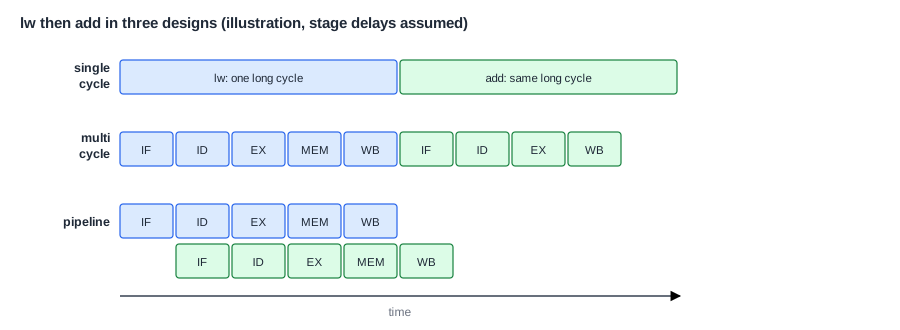
Take a program with an assumed mix of 25 percent loads, 10 percent stores, 50 percent arithmetic and 15 percent branches. The average number of cycles is 0.25 x 5 + 0.10 x 4 + 0.50 x 4 + 0.15 x 3 = 4.1. The time per instruction is 4.1 x 2 ns = 8.2 ns.
That is a surprise. The clock is four times faster than in the single-cycle design, but the average time per instruction is slightly longer, 8.2 ns against 8 ns. Two things went wrong. The steps do not take equal time, so the 1 ns steps waste half of their 2 ns cycle. And each register between steps adds a small delay of its own, which this calculation ignored. A load now takes 10 ns rather than 8 ns.
The multi-cycle design has real advantages, though. It removes the worst of the slow-path problem: a slow rare instruction can simply take more cycles, without slowing the clock. This is how early processors handled complex instructions, and it is why multiply and divide units still work this way today. And it can share hardware. Because only one step runs at a time, a single memory can serve both fetches and loads, and a single adder can serve the ALU and the program counter. Early computers, for which every gate was expensive, relied on this.
Sharing has a price of its own. The control logic is no longer a simple decoder: it is a state machine that must remember which step each instruction has reached, and every shared block needs multiplexers in front of it to choose its inputs. In a small design these extras are cheap compared with a second memory or a second adder, which is why the trade was so attractive when gates were expensive.
How the Two Compare on a Real Program
A very short program that prints a greeting shows the cycle counts. It executes about 200 instructions. On a single-cycle design that is about 200 cycles, on a multi-cycle design that needs five cycles per instruction about 1,000. A five-stage pipeline needs about 280. So the pipeline needs 1.4 times the cycles of the single-cycle design, at a clock that could be several times faster. The rest of this chapter explains where the extra 40 percent comes from, and how it is kept so small.
Where Is This Used?
The smallest processors really are built this way. Very small RISC-V cores for control tasks, such as those that manage power on a large chip, often take several cycles per instruction to save area, sometimes even working on a few bits at a time. A few gates and low power matter more there than speed. Single-cycle designs are common in teaching and in very slow embedded cores, where the clock is far below what the memory can handle anyway.
The Waste That Remains
Look at the multi-cycle design from the point of view of the hardware. While an instruction is in its execute step, the instruction memory, the decoder and the register file are all doing nothing. Each circuit works for one cycle out of four or five. So most of the chip is idle most of the time, in both designs.
The obvious question is: why wait? When the first instruction moves from fetch to decode, the fetch hardware is free. It could start the next instruction right away. Each block of hardware could be working on a different instruction at the same moment. That is a pipeline.
With the same 2 ns clock, a pipeline could finish one instruction every 2 ns, four times the rate of the multi-cycle design, using about the same hardware. It adds registers between the stages and some control logic, and it has problems of its own, because instructions now depend on each other while they overlap. Those problems are explained in The 5-Stage Pipeline. The idea, though, is so powerful that nearly every processor made since the 1980s uses it.
Quick Check
Q: With the delays in this article, what is the ideal time per instruction for each of the three designs: single-cycle, multi-cycle with the assumed mix, and a pipeline with a 2 ns clock that finishes one instruction per cycle?
Show Answer
Single-cycle: 8 ns. Multi-cycle: 8.2 ns. Pipeline: 2 ns. In real designs the pipeline loses some of that to hazards and register overhead, but it stays far ahead of the other two.
Latency and Throughput
These comparisons rest on two different ideas. Latency is how long one instruction takes from start to finish. Throughput is how many instructions finish per second. In the single-cycle design the two are tied together: one instruction takes one cycle, and one finishes each cycle. In a pipeline, they come apart. Each instruction still takes five stages, 10 ns, which is longer than the single-cycle 8 ns. But one finishes every 2 ns. Programs care about throughput, because a program is millions of instructions in a row, so a longer latency for each instruction is a price worth paying.
Common Mistakes
Mistake #1: Judging a design by its clock frequency
The multi-cycle design has a clock four times faster than the single-cycle design and does not run programs faster. Only cycles multiplied by the period counts, as The Performance Equation explains.
Mistake #2: Assuming a CPI of 1 means the design is fast
The single-cycle design has a perfect CPI of 1, and it is the slowest clock in the comparison. A CPI is only meaningful together with the clock period it was achieved at.
Mistake #3: Forgetting that the steps are unequal
Dividing 8 ns of work into 5 steps does not give a 1.6 ns clock, because the clock must fit the longest step. Balancing the steps is one of the main jobs in designing a pipeline.
Practice Exercise
Challenge: A New Instruction Mix
Using the step delays in this article, assume a program of 40 percent loads, 10 percent stores, 30 percent arithmetic and 20 percent branches. (a) What is the time per instruction on the single-cycle design? (b) What is the average CPI and the time per instruction on the multi-cycle design? (c) Register overhead adds 0.2 ns to each multi-cycle clock period. What is the time per instruction now? (d) Which design wins?
Hint
The single-cycle clock does not depend on the mix. The multi-cycle clock is the longest step, plus overhead for part (c).
Solution
(a) 8 ns, unchanged. (b) CPI = 0.4 x 5 + 0.1 x 4 + 0.3 x 4 + 0.2 x 3 = 2.0 + 0.4 + 1.2 + 0.6 = 4.2, so 4.2 x 2 ns = 8.4 ns. (c) 4.2 x 2.2 ns = 9.24 ns. (d) The single-cycle design is faster for this program, by about 15 percent. The multi-cycle design only wins when instructions need very different amounts of time, for example with a slow memory or long multiply operations.
Summary
- A single-cycle processor finishes every instruction in one clock cycle, but that cycle must fit the slowest instruction.
- A multi-cycle processor uses short cycles and varying cycle counts, and shares hardware between the steps.
- With unequal steps and register overhead, the multi-cycle design is often no faster than the single-cycle one.
- In both designs most of the hardware is idle most of the time.
- A pipeline overlaps instructions so that every block stays busy, trading a little latency for a large gain in throughput.
