
RTL sign-off means verification of the design description is complete. Tapeout means the physical chip data is being sent to the semiconductor foundry for fabrication — and that step is irreversible. The gap between these two milestones is where a final, focused set of verification activities takes place to confirm that nothing was lost or corrupted in the journey from RTL to silicon-ready layout. This article walks through each of those steps.
11 min read | Intermediate Level
What You'll Learn
- Why gate-level simulation is needed even after RTL sign-off
- What SDF back-annotation is and what timing failures it can expose
- What DRC and LVS check and why they are sign-off gates
- How configuration verification prevents the wrong RTL from being taped out
The Gap Between RTL Sign-Off and Tapeout
RTL simulation operates on an idealised model of the design — logic with no physical delay, wires with no resistance or capacitance, and flip-flops that switch in exactly zero time. The real chip that comes back from the foundry operates under none of these assumptions. Synthesis maps the RTL to actual logic gates, place and route arranges those gates on silicon and connects them with real metal wires, and the resulting circuit has propagation delays, crosstalk, and timing constraints that simulation never saw.
The tapeout verification steps exist to bridge that gap — to check that the implementation of the design is as functionally correct as the RTL description of it.
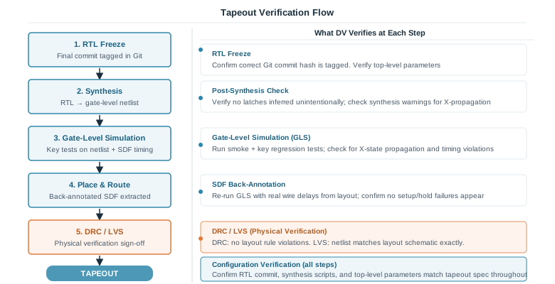
Step 1 — RTL Freeze and Configuration Verification
In practice, physical implementation does not wait for every last line of RTL to be finalised. Physical design (PD) typically begins picking up RTL drops incrementally — once the major blocks are stable and the top-level architecture is locked, the PD team starts floorplanning and early placement even while smaller RTL fixes are still being integrated. What changes at the tapeout milestone is that a specific Git commit is tagged as the final baseline, after which no further RTL changes are permitted without a formal change control process. This final freeze is what the gate-level simulation and sign-off regression are run against — it is the foundation on which the last verification steps rely.
Configuration verification runs in parallel with every step that follows. It answers a deceptively simple question: is the right RTL actually being used? In a large SoC project, dozens of IP blocks each have their own repositories, parameter sets, and revision histories. A mismatch — the wrong commit hash, a stale parameter, a block compiled with debug features left enabled — can survive all the way to tapeout if nobody explicitly checks.
Document the expected Git commit hash, top-level parameter values, and synthesis script version in the tapeout checklist before any physical implementation begins. Re-verify all three at the end of the flow before the tapeout data is released to the foundry.
Common configuration checks include: confirming that scan insertion and BIST (Built-In Self-Test) modes are correctly enabled or disabled, verifying that any design-for-test logic is in its intended state, and confirming that memory compiler versions and standard cell libraries match the versions used in sign-off simulation.
Step 2 — Synthesis and Post-Synthesis Checks
Synthesis converts the RTL into a gate-level netlist — a description of the design using only the actual logic cells available in the target technology library (AND gates, flip-flops, multiplexers, and so on). The DV team is not responsible for running synthesis, but they do care about its output for two reasons.
First, synthesis tools emit warnings that can indicate functional problems. An unintended latch inferred from an incomplete if statement, a combinational loop, or a multi-driven net are all synthesis warnings that can produce functional bugs in the gate-level netlist that were not present at RTL level. The DV engineer reviews these warnings alongside the design team.
Second, synthesis may perform optimisations — constant propagation, logic merging, redundant logic removal — that change the structure of the circuit without changing its function. Confirming this through gate-level simulation (the next step) catches cases where an optimisation was applied incorrectly.
A synthesis warning is not automatically a bug, but it is always worth investigating. Warning categories like "latch inferred for signal X" or "combinational loop detected" require explicit sign-off from the design team before the netlist is used for gate-level simulation.
Step 3 — Gate-Level Simulation (GLS)
Gate-level simulation (GLS) re-runs a subset of the verification tests — typically the smoke tests and the most functionally critical regression tests — against the synthesised netlist rather than the RTL. The testbench is the same; only the design under test changes from the RTL model to the gate-level netlist.
GLS serves two purposes. The first is functional correlation: confirming that the gate-level netlist produces the same outputs as the RTL for the same inputs. If synthesis introduced a functional bug — a dropped signal, a timing path that doesn't exist in RTL, or an incorrectly optimised logic cone — GLS will surface it.
The second purpose is X-state propagation checking. In RTL simulation, uninitialised signals are represented as X (unknown). RTL simulators often mask X propagation — an X going into a multiplexer may produce a valid output if the select line is known. Gate-level simulators propagate X more aggressively through the actual cell models, which can expose initialisation problems that were hidden at RTL level.
Running the full regression suite on the gate-level netlist is typically impractical — GLS is orders of magnitude slower than RTL simulation because every gate switch must be modelled individually. The selection of which tests to run is therefore critical: choose tests that cover the most functionality per simulation minute, prioritising reset sequences, key protocol transactions, and any tests that previously found bugs.
Step 4 — SDF Back-Annotation and Timing Verification
After place and route is complete, the physical implementation tools extract a Standard Delay Format (SDF) file. This file contains the actual propagation delays for every gate and wire in the design, calculated from the real layout geometry and the foundry's timing models. Back-annotation means loading this SDF file into the gate-level simulator alongside the netlist, so that the simulation now models real timing rather than zero-delay logic.
GLS with SDF back-annotation is the closest a pre-silicon simulation gets to the behaviour of the real chip. At this stage, the simulator can detect setup time violations — where a signal arrives at a flip-flop too late relative to the clock edge — and hold time violations — where a signal changes too soon after the clock edge and the flip-flop cannot reliably capture the correct value.
Quick Check
Q: GLS without SDF passes all tests. GLS with SDF back-annotation produces a timing violation on a data path leading to a register in the memory controller. What does this mean, and is it a DV problem or a physical design problem?
Show Answer
It means that after place and route, the wire delay on that path is long enough that the signal does not reach the register's data input before the clock edge — a setup time violation. This is primarily a physical design (PD) problem: the tool did not achieve timing closure on that path. However, it is also a DV concern because if it is not fixed before tapeout, the chip may malfunction at the target clock frequency. DV's role is to flag the violation and ensure it is either fixed in the layout or that a formal timing exception (a waiver approved by the design lead) is applied with full understanding of the functional impact.
Timing sign-off is primarily owned by the physical design and timing analysis teams using static timing analysis (STA) tools, which exhaustively check every path without needing to simulate. GLS with SDF provides a dynamic confirmation of timing — it can only check the paths that the simulation stimulus actually exercises, making STA the authoritative sign-off tool and GLS a corroborating check.
Step 5 — DRC and LVS
Design Rule Check (DRC) and Layout Versus Schematic (LVS) are physical verification steps that check the layout database — the geometric description of the chip that the foundry will use to manufacture it.
Design Rule Check (DRC)
DRC verifies that the physical layout obeys the foundry's manufacturing rules. These rules govern things like the minimum width of a metal wire, the minimum spacing between adjacent wires, and the minimum overlap between a contact and the layer it connects to. Violating a design rule can cause the chip to fail during manufacturing or produce a circuit with higher defect rates.
DRC is entirely outside the scope of functional verification — it operates on the geometric layout database, not on logic or signal behaviour. It is owned and run by the physical design team. It is included here because DV engineers need to understand what it is and why a DRC failure can block tapeout and trigger downstream re-work that may require gate-level simulation to be re-run.
Layout Versus Schematic (LVS)
LVS compares the physical layout against the gate-level netlist to confirm they describe the same circuit. An LVS failure means there is a discrepancy between what the layout shows and what the netlist specifies — a net that is connected in the netlist but not in the layout, or a transistor that is sized differently. Like DRC, LVS is owned by the physical design team and sits outside the scope of functional verification. LVS failures must reach zero before tapeout: sending a layout that does not match the verified netlist to the foundry would mean fabricating a different circuit from the one that was simulated and signed off — making all pre-silicon verification effort meaningless for that chip.
DRC and LVS are sometimes collectively called physical verification or signoff checks. Both must pass with zero errors — not "mostly clean" — before the chip data is released to the foundry. Most companies have a dedicated physical verification team who own these checks, but the results feed back into DV sign-off documentation.
Step 6 — The Final Regression Run
The last DV action before tapeout approval is running the complete sign-off regression suite one final time, against the frozen RTL commit and using the same simulation environment that was used for RTL sign-off. This run confirms that nothing in the post-sign-off activity — configuration changes, parameter updates, test infrastructure modifications — has inadvertently broken any previously passing tests.
The result of this run, along with the RTL commit hash, the synthesis script version, and the SDF file version, is recorded in the tapeout sign-off package — the formal documentation that authorises the tapeout. This package is archived permanently; if a post-silicon bug is found months later, the sign-off package is the reference that allows the team to reconstruct exactly what was verified and with what tools.
Run the final regression with verbosity logging enabled and save the complete simulation logs. If a post-silicon escape requires correlation back to pre-silicon simulation later, having the original log files alongside the sign-off package saves significant debug time.
What DV Does Not Own at Tapeout
It is worth being clear about boundaries. The DV team owns functional correctness — the design does what the specification says. The physical design team owns timing closure (STA), layout correctness (DRC/LVS), and power grid integrity. The design team owns the RTL and synthesis scripts. At tapeout, all three teams sign off independently, and the project manager or chip lead collects all three sign-offs before releasing to the foundry.
A DV engineer who is asked to sign off on a tapeout package is confirming: the correct RTL was used, the sign-off regression passed, gate-level simulation showed functional correlation, and the SDF-annotated simulation raised no unresolved timing failures in paths exercised by the tests. They are not confirming that the layout is physically correct — that is the physical design team's accountability.
Quick Check
Q: The physical design team reports that LVS is clean but DRC has five remaining violations on metal layer 3 spacing, all in a corner of the chip far from any functional logic. The tapeout deadline is tomorrow. Should the DV team sign off on the tapeout package?
Show Answer
DRC violations are not DV's direct accountability, but the DV team should not sign off on a tapeout package until the DRC status is resolved or formally waived by the physical design lead and chip lead. "Far from any functional logic" is not a rigorous engineering justification — DRC rules exist because foundry processes are not perfectly predictable, and a spacing violation anywhere on the chip increases manufacturing defect risk. The correct action is to escalate to the chip lead, not to proceed and hope the violations are benign.
Common Mistakes
Mistake 1: Assuming RTL sign-off means tapeout verification is complete.
Wrong: After RTL sign-off is granted, no further DV activity is performed before tapeout.
Right: RTL sign-off closes pre-silicon functional verification. Gate-level simulation, SDF timing correlation, and the final regression run are separate steps that must still be completed.
Why? Synthesis and place and route can introduce functional bugs that were not present at RTL level — unintended latches, incorrectly optimised paths, or X-propagation issues hidden by RTL simulation semantics. GLS is the check that catches these.
Mistake 2: Running GLS with zero-delay (no SDF) and treating it as equivalent to back-annotated GLS.
Wrong: Reporting "GLS passed" based on zero-delay simulation and not following up with SDF back-annotation.
Right: Zero-delay GLS checks functional correctness of the netlist. SDF back-annotation additionally checks timing. Both are needed; zero-delay GLS alone cannot detect setup or hold violations.
Why? A design can be functionally correct in zero-delay simulation but fail timing in silicon if physical routing introduced delays that the logic was not designed to tolerate. Zero-delay GLS cannot see these delays because it ignores them by definition.
Mistake 3: Not archiving the tapeout sign-off package with full simulation logs.
Wrong: Recording only a pass/fail summary in the tapeout documentation without saving the actual simulation logs or the SDF file used.
Right: Archive the complete regression logs, the SDF file, the synthesis netlist, the Git commit hash, and all waiver documentation together as a single tapeout package.
Why? Post-silicon escapes are sometimes investigated months or years after tapeout. Without the original simulation logs and configuration files, it is impossible to determine whether a silicon bug was a verification gap or a post-silicon-only effect. The archive is the evidence.
Practice Exercise
Challenge: Triage a Tapeout Readiness Review
Your chip lead sends the following tapeout readiness status one day before the scheduled release:
- RTL commit
b2e9f4atagged as tapeout baseline - Synthesis completed — two warnings: "latch inferred for signal
cfg_mode" and "unused input on cell U4471" - Zero-delay GLS passed all smoke tests
- SDF back-annotated GLS not yet run — physical team says "layout just finished, SDF available tomorrow"
- DRC: clean. LVS: clean
- Final regression: not yet run against commit
b2e9f4a— last regression run was againstb2e9f1c(three commits ago)
Identify which items are clear, which are blockers, and what actions are needed before tapeout can proceed.
Hint
Work through each item against the checklist in this article. Pay attention to the synthesis warning about the latch and the gap between the regression commit and the tapeout commit.
Sample Answer
Clear:
- RTL commit tagged — clear.
- Zero-delay GLS passed — provides functional netlist correlation.
- DRC and LVS clean — physical verification is clear.
Blockers:
1. Synthesis warning — latch inferred for cfg_mode: This is a potential functional bug. An unintended latch on a configuration signal can cause the chip to behave unpredictably depending on when power-up initialisation occurs. The design team must confirm whether this latch is intentional. If it is not, the RTL must be fixed and synthesis re-run before tapeout.
2. SDF back-annotated GLS not run: This is a hard blocker. Zero-delay GLS cannot detect timing violations. With the SDF available tomorrow, this should be run and reviewed before tapeout is approved — a one-day delay is far preferable to a post-silicon timing failure.
3. Final regression not run against the tapeout commit: The last regression was three commits ago. Those three commits may include changes that introduced regressions. The final regression must be re-run against b2e9f4a before sign-off.
Investigate but not necessarily a blocker:
- "Unused input on cell U4471" synthesis warning: this is typically a minor warning (a floating input tied to a valid logic level by the synthesis tool), but it should be confirmed with the design team that the cell in question is not on a critical path.
Summary
In this article, you learned:
- Tapeout verification bridges the gap between RTL sign-off and the physical chip — synthesis and layout can introduce bugs that RTL simulation never sees
- Gate-level simulation re-runs key tests on the synthesised netlist to confirm functional correctness and catch X-propagation issues
- SDF back-annotation loads real wire delays into GLS, enabling detection of setup and hold time violations introduced by physical routing
- DRC confirms the layout obeys foundry manufacturing rules; LVS confirms the layout matches the verified netlist — both must be zero-error before tapeout
- Configuration verification and a final regression run against the tagged tapeout commit are the last DV actions before the sign-off package is released to the foundry
