
Most of this tutorial series has focused on the technical side of verification — testbenches, coverage, assertions, and simulation. But verification does not happen in isolation. It is a team activity, and understanding who does what, how the DV engineer interacts with the RTL design team, and where a career in verification can lead is essential knowledge before stepping into an industry role. This article maps out the landscape.
10 min read | Intermediate Level
What You'll Learn
- What a DV engineer does day-to-day and how it differs from an RTL design role
- Where the two roles collaborate and what each is accountable for
- The career paths available within the verification discipline
- The skills that distinguish a strong DV engineer from a competent one
The Core Distinction
The RTL design engineer and the DV engineer share a common goal — a working chip — but they approach it from opposite directions. The design engineer asks: "How do I build this?" The DV engineer asks: "How do I prove this works?" This adversarial mindset is not accidental. A DV engineer who simply trusts the RTL is not doing their job. Their role is to find every way the design can fail before silicon is made.
In many companies, DV and design roles are filled by different people with different backgrounds. In smaller teams, one engineer may do both. Either way, keeping the responsibilities distinct — even mentally — is important. A design engineer reviewing their own RTL for bugs is far less effective than an independent DV engineer doing the same job, because the designer's mental model of the design already contains the same assumptions that caused the bug.
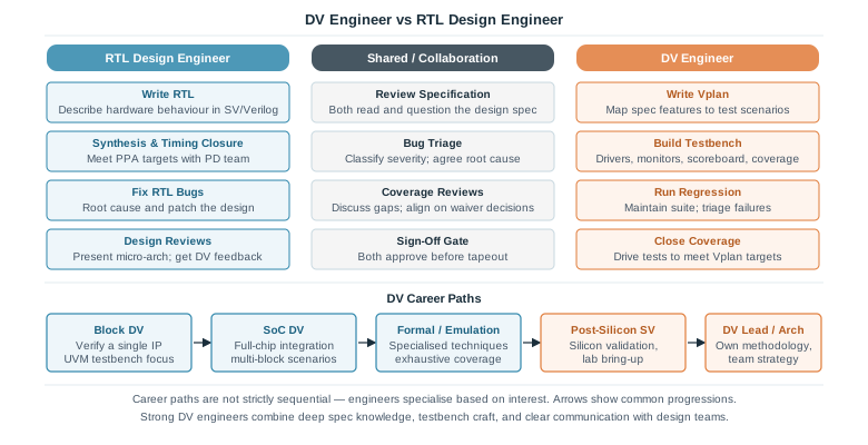
What a DV Engineer Does Day-to-Day
The day-to-day work of a DV engineer varies by project phase, but the recurring activities across a typical week look like this:
Writing and Maintaining the Verification Plan
Early in the project, the DV engineer reads the design specification and produces the Vplan — a document mapping every design feature to a set of test scenarios, coverage points, and pass/fail criteria. This is not a one-time task. As the specification evolves and new features are added, the Vplan must be updated to stay in sync. A stale Vplan is a coverage gap waiting to cause an escape.
Building and Extending the Testbench
The testbench infrastructure — drivers, monitors, scoreboards, coverage collectors, and constraint models — is the DV engineer's primary deliverable. In most industry projects this means building a UVM environment, though the complexity varies from a simple block-level testbench to a multi-agent SoC environment with VIP (Verification IP) from third-party vendors. Testbench development is real software engineering: it requires thoughtful architecture, code review, and maintenance.
Running Regression and Triaging Failures
Regression runs — typically launched nightly against the latest RTL — produce a pass/fail report that the DV engineer triages each morning. Not every failure is an RTL bug. Some are testbench issues, some are infrastructure problems, some are known issues already in the tracker. The DV engineer must quickly separate real RTL bugs from noise and keep the regression suite trustworthy.
Closing Coverage
Coverage dashboards are reviewed regularly. Uncovered bins and low-coverage blocks are prioritised, and new tests or tighter constraints are written to close the gaps. Coverage closure is often the most time-consuming phase of a project — the last 5% of functional coverage frequently requires more effort than the first 90%.
Filing and Tracking Bugs
When a genuine RTL bug is found, the DV engineer files a clear, reproducible bug report (as covered in article 7.1) and tracks it through triage, fix, retest, and closure. Communication quality matters here — a vague bug report costs time for the design team and reflects poorly on the DV process.
Quick Check
Q: A nightly regression run produces 12 new failures. The DV engineer checks and finds 9 are caused by a missing wait statement in the testbench reset sequence that broke after a recent testbench commit, 2 are known bugs already in the tracker, and 1 is a genuine new RTL failure. What should the DV engineer do for each category?
Show Answer
The 9 testbench failures need an immediate fix to the testbench reset sequence — these should not be filed as RTL bugs. The 2 known bugs are already tracked; no new action needed unless they have changed in character. The 1 genuine RTL failure should be confirmed as reproducible, then filed as a new bug with the simulation command, seed, expected vs observed behaviour, and RTL commit hash. The regression should be re-run after the testbench fix is committed to establish a clean baseline.
What an RTL Design Engineer Does
The RTL design engineer is responsible for translating the design specification into synthesisable hardware description. Their primary deliverables are the RTL source files — the SystemVerilog or Verilog that describes the chip's behaviour. Beyond writing RTL, the design engineer is responsible for:
- Microarchitecture definition: Deciding how the high-level specification maps to actual hardware structures — pipelines, state machines, FIFOs, arbiters
- Synthesis and timing closure: Working with the physical design team to ensure the RTL meets PPA (Performance, Power, Area) targets after synthesis and place-and-route
- RTL bug fixing: Owning the root cause analysis and fix for bugs filed by the DV team, and providing clear explanations of what changed and why
- Design reviews: Presenting the microarchitecture to peers and the DV team for early feedback before RTL is written
A key distinction from software development: the RTL design engineer must think in hardware. Parallel execution, clock edges, reset states, synthesis implications, and timing paths are constant considerations. Code that looks correct to a software developer may infer unintended latches or create combinational loops in hardware.
Where the Two Roles Collaborate
DV and design engineers interact at several well-defined points throughout the project. Each of these touchpoints is an opportunity for quality improvement — and a failure point if communication breaks down.
Specification Review
Before any RTL or testbench is written, both engineers read the design specification. The DV engineer is often the first to catch ambiguities — because they are thinking about how to test every case, they ask questions like "what happens if reset is asserted mid-transaction?" or "is this field writable or read-only?" that the design engineer may not have considered. Resolving these ambiguities early prevents both incorrect RTL and incorrect testbench assumptions.
Design Reviews
Microarchitecture design reviews are typically attended by both roles. The DV engineer's job in a design review is not to rubber-stamp the design but to ask testability questions: are there enough debug observability hooks? Is the reset sequence deterministic enough to be simulated reliably? Are there internal signals that the scoreboard will need to observe?
Bug Triage and Discussion
When a bug is filed, the DV engineer and the design engineer often discuss it directly before formal triage. The DV engineer provides the reproducer; the design engineer provides early insight into which code path is likely responsible. This informal communication — done well — shortens the triage-to-fix cycle significantly.
Coverage Reviews
Mid-project coverage reviews bring both roles together to assess progress. The design engineer can often clarify which uncovered bins are genuinely unreachable (and should be waived) versus which represent real untested scenarios. This saves the DV engineer from spending days writing tests for scenarios that the design physically cannot enter.
The relationship between DV and design engineers works best when it is collaborative rather than adversarial in a negative sense. The DV engineer's job is to find bugs — but the goal is not to "catch" the design engineer making mistakes. The goal is to ship a chip that works. Both roles share that objective, and teams that operate with mutual respect and open communication consistently produce better results.
Career Paths in Verification
Verification is a broad discipline with several distinct specialisations. Most DV engineers begin at the block level and develop expertise across one or more of the following paths over time.
Block-Level DV
The entry point for most DV engineers. Responsible for verifying a single IP block — an AXI interconnect, a memory controller, a crypto accelerator — in isolation. Requires deep knowledge of the block's specification, the testbench methodology (typically UVM), and the tools used for simulation and coverage analysis. This is where testbench engineering skills are developed.
SoC-Level DV
SoC DV involves verifying the full chip — all blocks connected together — and is significantly more complex than block-level DV. The focus shifts from individual block behaviour to integration correctness: address map verification, interrupt routing, DMA transfers across multiple bus masters, power sequencing across domains. SoC DV engineers typically work with many IPs simultaneously and coordinate with multiple block DV teams.
Formal Verification
Formal verification uses mathematical proof rather than simulation to exhaustively check design properties. Formal engineers write properties in SVA and use tools (Cadence JasperGold, Synopsys VC Formal) to prove them over all possible inputs. Formal is particularly powerful for control logic, protocol checkers, and reset behaviour — scenarios where simulation's random coverage is slow and unreliable. This is a specialised track requiring strong knowledge of SVA and formal tool flows.
Emulation
Hardware emulation runs RTL on a reprogrammable hardware platform (such as Cadence Palladium or Synopsys ZeBu) at speeds far faster than software simulation. Emulation engineers set up the emulation environment, debug bring-up issues specific to the emulation platform, and run software stacks and firmware against the design long before silicon arrives. This role bridges DV and post-silicon validation.
Post-Silicon Validation
Silicon validation (SV) engineers work in the hardware lab, running validation tests on real chips. The skills overlap significantly with DV — reading specifications, writing test plans, triaging failures — but the tools and environment are entirely different: oscilloscopes, logic analysers, JTAG, and custom lab automation scripts rather than simulation waveforms. Post-silicon validation experience is highly valued and often leads to senior technical roles.
DV Lead and Methodology Architect
Senior DV engineers often move into lead roles, owning the verification strategy for an entire chip or product line. DV leads write the top-level Vplan, define the testbench architecture, mentor junior engineers, run coverage and sign-off reviews, and represent DV in project management discussions. Above that, methodology architects define the tools, flows, VIP strategy, and standards used across multiple chip projects or across the company.
Quick Check
Q: A DV engineer is asked to join a formal verification effort for the first time. They are comfortable with UVM testbenches and constrained-random simulation. What is the most important new skill they need to develop?
Show Answer
Writing SVA properties and understanding how formal tools consume them. Constrained-random simulation generates stimulus and checks outputs dynamically — formal verification works by statically proving that a property holds for all possible inputs. The DV engineer needs to learn to express design intent as precise mathematical properties (using SVA assert, assume, and cover constructs) and understand how to interpret formal tool output: proven, falsified, or inconclusive (vacuous) results. The testbench engineering skills from UVM are largely not transferable — formal has a completely different workflow.
Skills That Distinguish a Strong DV Engineer
Technical skills — SystemVerilog, UVM, assertions, coverage — are the baseline. What separates a strong DV engineer from a competent one is a combination of qualities that go beyond tool knowledge.
Deep Specification Reading
The best DV engineers read a specification and immediately see the edge cases, the underspecified behaviour, and the scenarios that will be hardest to test. This is a skill developed over time and across many projects. It requires patience, scepticism, and genuine curiosity about how things can go wrong.
Testbench Architecture Judgment
A testbench that is difficult to extend, hard to debug, or slow to run wastes time for the entire team. Strong DV engineers design testbenches with reuse, maintainability, and simulation performance in mind — not just correctness for the immediate project.
Debugging Skill
Simulation failures are rarely self-explanatory. Tracing a scoreboard mismatch backward through a pipeline, identifying the root cause of an assertion firing, or isolating a race condition that only appears with one seed in ten thousand — these require methodical, patient debug skills. Strong DV engineers are comfortable in the waveform viewer and know how to bisect a problem efficiently.
Communication
DV engineers write bug reports that design engineers must act on, present coverage status to project managers, and argue for schedule time to close verification gaps. Written clarity, technical precision, and the ability to summarise complex simulation data in a few sentences are practical daily requirements — not soft skills sitting at the side of the job.
Scepticism About Their Own Testbench
A DV engineer whose scoreboard always passes should be suspicious, not satisfied. A testbench that never finds bugs may be a testbench that cannot find bugs. Actively looking for weaknesses in the verification environment — checking that the scoreboard genuinely fails when it should, that coverage bins are sampling correctly, that constraint solvers are not trivially satisfying constraints — is a mark of a mature verification engineer.
One of the best habits a new DV engineer can develop is deliberately injecting a known bug into the RTL and confirming that the testbench catches it. If it does not, the coverage model or checker has a gap. This practice — sometimes called fault injection testing of the testbench itself — builds confidence that the environment actually works.
Common Mistakes
Mistake 1: Treating the testbench as less important than the RTL.
Wrong: Rushing the testbench together quickly to start running tests, treating architecture and maintainability as things to fix later if there is time.
Right: The testbench is a long-lived engineering artefact. A poorly architected testbench that is hard to extend will slow down coverage closure and make bug investigation harder for the entire project duration.
Why? In a six-month verification project, a testbench written in the first two weeks will be modified, debugged, and extended for the remaining four. Poor initial design compounds into lost time every week.
Mistake 2: Only communicating with the design team through the bug tracker.
Wrong: Filing bugs and waiting for responses without any direct discussion, treating the bug tracker as the only interface with the RTL design team.
Right: Regular informal communication — discussing a failing test directly with the designer, attending design reviews early, asking questions during spec review — surfaces problems faster and builds the working relationship that makes triage efficient.
Why? Many bugs that take days to resolve through ticket comments are resolved in a ten-minute conversation. The bug tracker records decisions; it does not replace engineering communication.
Mistake 3: Assuming a passing regression means the design is correct.
Wrong: Reporting "regression is green" as evidence that verification is complete.
Right: A green regression means the existing tests pass. It says nothing about the scenarios those tests do not cover. Coverage closure is the measure of verification completeness — regression green is a necessary condition, not a sufficient one.
Why? A testbench that only tests the happy path will always have a green regression. The uncovered error-handling paths, corner cases, and protocol edge cases are exactly where real chips fail in silicon.
Practice Exercise
Challenge: Assign Responsibilities
A new chip project is starting. The following tasks need to be assigned to either the RTL design engineer (DE), the DV engineer (DV), or both jointly (Both). Assign each task and briefly justify your answer.
- Read the specification and identify ambiguous or underspecified behaviour
- Decide whether a specific uncovered coverage bin should be waived or tested
- Write the AXI slave interface RTL
- Write the AXI protocol checker assertion in SVA
- Determine the root cause of a scoreboard mismatch at simulation time 14,500 ns
- Commit a fix for an RTL bug where the FIFO write pointer increments incorrectly
- Confirm the bug fix did not break any previously passing tests
Show Answer
1. Both. Both roles read the spec and bring different perspectives — DE looks for implementability, DV looks for testability and edge cases.
2. Both jointly. The DE clarifies whether the scenario is physically reachable; the DV engineer owns the coverage decision and files the waiver. Neither should decide alone.
3. DE. Writing RTL is the design engineer's primary deliverable.
4. DV. Protocol checkers are testbench infrastructure — they belong to the DV engineer. The DE may review them to confirm correctness against the spec.
5. Both. The DV engineer traces the simulation failure and provides the reproducer; the DE identifies which RTL path is responsible. In practice both engineers often debug together.
6. DE. Only the design engineer should modify and commit RTL fixes. DV engineers do not edit the design source.
7. DV. Retest and regression are owned by the DV engineer. The DE confirms the fix logic; the DV engineer confirms it passes all tests.
Summary
In this article, you learned:
- The RTL design engineer builds the hardware; the DV engineer proves it works — both roles are essential and complementary, not interchangeable
- DV day-to-day work spans Vplan writing, testbench development, regression triage, coverage closure, and bug tracking
- Key collaboration touchpoints are specification review, design reviews, bug triage, and coverage reviews — communication quality at these points directly affects project quality
- Verification careers can develop through block DV, SoC DV, formal verification, emulation, post-silicon validation, and into DV lead and methodology roles
- The strongest DV engineers combine specification reading depth, testbench architecture judgment, systematic debug skill, and clear technical communication