
Pre-silicon verification, no matter how thorough, operates on a model. The real chip that comes back from the foundry is a physical object — it runs at voltage, heats up, has wires with real resistance, and will eventually sit inside a product being used by a customer in conditions that no simulation ever modelled. Post-silicon validation is the process of testing that physical chip to confirm it works correctly in the real world. This article explains what that process looks like, how it differs from simulation, and how failures found at this stage feed back into improving pre-silicon verification on the next design.
12 min read | Intermediate Level
What You'll Learn
- What silicon bring-up is and what the team checks at each stage
- Why silicon behaves differently from simulation and what effects simulation cannot model
- What hardware debug tools are used when a chip fails in the lab
- How post-silicon escapes feed back into the pre-silicon verification plan
Who Does Post-Silicon Validation?
Post-silicon validation is carried out by a dedicated silicon validation (SV) team, separate from the design verification (DV) team that ran pre-silicon simulation. The SV engineer works in a hardware lab — with physical boards, test equipment, and prototype chips — rather than at a simulation workstation. Despite the different environment, the mindset is similar: apply stimulus, observe outputs, compare against specification, and investigate anything that deviates.
Pre-silicon DV engineers are often involved in post-silicon validation, particularly in smaller teams. Familiarity with the design specification, the verification plan, and the testbench helps considerably when correlating a silicon failure back to a simulation scenario.
The Silicon Bring-Up Process
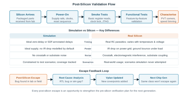
Bring-up refers to the process of powering on a new chip for the first time and progressively proving that it works. It follows a structured sequence, moving from the most basic checks to increasingly complex functional tests.
Step 1 — Power-On and Supply Verification
Before any logic is exercised, the validation engineer verifies that all power supply rails are at the correct voltages, current draw is within expected limits, and no short circuits exist. A chip drawing far more current than expected at power-on is a signal of a physical fault — a short in the power grid or a catastrophic synthesis error — and no further testing proceeds until the power profile is understood.
Step 2 — Clock and Reset Bring-Up
Once power is stable, the team brings up the clock sources and exercises the reset sequence. A Phase-Locked Loop (PLL) locking to the reference clock is one of the first functional milestones — without a locked clock, no synchronous logic operates correctly. Reset de-assertion timing is also verified to confirm that all blocks initialise to their documented reset state.
The reset sequence in silicon is often the first place where differences from simulation appear. Simulation typically uses an ideal reset pulse with precise timing. In silicon, reset de-assertion interacts with PLL lock time, power-on-reset circuits, and real clock edges — small timing differences can leave registers in unexpected states that simulation never exercised.
Step 3 — Smoke Tests
With power and clocks confirmed, the team runs the simplest possible functional checks: reading known-good registers over JTAG, verifying that device identification registers return the correct values, and confirming that basic communication interfaces (UART, SPI, I2C) respond. These tests are the hardware equivalent of RTL simulation smoke tests — they confirm the chip is alive and responsive before investing time in complex test sequences.
Step 4 — Functional Validation
Once smoke tests pass, the team works through the full feature set methodically, following a validation plan analogous to the pre-silicon Vplan. Each feature is exercised, outputs are compared against specification, and any deviation is logged as a bug. This phase is where the majority of post-silicon bugs are discovered — and where the differences between simulation and silicon matter most.
Step 5 — Characterisation
After functional validation, the chip is characterised across its full operating range: supply voltage variation (across the specified voltage range), temperature extremes (from cold to hot), and multiple silicon samples from different manufacturing lots. Characterisation confirms that the design operates correctly not just under nominal conditions, but across the process, voltage, and temperature (PVT) corners. Speed binning — testing which chips can run at higher clock frequencies — is also performed here and feeds into product tier decisions.
How Silicon Differs From Simulation
Understanding why silicon can behave differently from simulation is important for any DV engineer, because it explains both where post-silicon escapes come from and why pre-silicon verification cannot catch everything.
Parasitics — Resistance and Capacitance of Wires
In RTL simulation, wires have no resistance or capacitance — signals propagate instantaneously unless SDF back-annotation is applied. In real silicon, every wire has a resistance and every junction has a capacitance. These parasitics create RC delays that slow signal propagation, cause voltage droop on long wires, and produce glitches at high switching frequencies. Even with SDF back-annotation, the delay models are approximations — silicon parasitics measured from an actual fabricated chip can differ from the models used during signoff.
Temperature and Voltage Variation
Transistor switching speed is a function of both temperature and supply voltage. A chip that passes timing at nominal voltage and room temperature may fail at low voltage (slow transistors) or high temperature (also slow transistors, due to reduced carrier mobility). Simulation runs at specific PVT corners, but silicon sees the full continuous range — including combinations that no simulation corner modelled exactly.
Crosstalk and Noise
When a signal switches on one wire, capacitive coupling injects a small voltage spike onto adjacent wires. If multiple wires switch simultaneously, this crosstalk can corrupt data on a nearby signal. Simulation does not model crosstalk unless a specific post-layout noise analysis is performed, which is typically run only on critical paths. In silicon, crosstalk is present everywhere and can cause failures on paths that were clean in simulation.
Real-World Usage Scenarios
Pre-silicon simulation operates within the bounds of the verification plan — the scenarios the team thought to test. A customer using the chip in a real product will encounter combinations of operating conditions, firmware sequences, and peripheral configurations that no simulation test ever attempted. This is the deepest fundamental difference: simulation is a closed world; silicon in a product is an open one.
Quick Check
Q: A chip passes all gate-level simulation tests with SDF back-annotation at the nominal PVT corner. In silicon bring-up, a timing failure appears at the high-temperature, low-voltage corner. Does this mean the pre-silicon verification team made a mistake?
Show Answer
Not necessarily. The SDF-annotated GLS run was at the nominal corner — it was not required to simulate the slow PVT corner unless that corner was specifically included in the sign-off regression plan. Timing failures at extreme PVT corners are primarily caught by static timing analysis (STA), which exhaustively checks all paths across all corners. If the STA signoff included the slow corner and showed it clean, the failure may indicate a modelling inaccuracy in the delay libraries. If the slow corner was not included in STA signoff, that is a process gap — a coverage hole in the physical design verification flow, not in functional DV.
Hardware Debug Tools
When a chip fails a silicon validation test, the debug environment is fundamentally different from simulation. There is no waveform viewer showing every internal signal — the validation engineer can only observe what the chip exposes at its pins and through its debug interfaces.
JTAG and Boundary Scan
JTAG (Joint Test Action Group) is a standardised serial interface built into almost every digital chip. It provides access to internal scan chains, allowing the validation engineer to read and write register values, run built-in self-test (BIST) routines, and exercise the chip's logic without needing external stimulus on every pin. JTAG is typically the first debug interface used after reset bring-up — if JTAG responds correctly, the team knows the core logic is alive and accessible.
Boundary scan uses the JTAG interface to test the connectivity of the chip's I/O pins — confirming that signals can be driven and observed at the package boundary without needing a full functional test sequence. This is particularly valuable for catching board-level wiring faults early in bring-up.
Logic Analysers
A logic analyser connects to the chip's output pins and captures digital signal transitions over time, building a waveform record similar to what a simulator would display — but limited to observable pins. Modern logic analysers can trigger on specific patterns, making it possible to capture the state of the bus at the exact moment a protocol violation occurs. The limitation is visibility: unlike simulation, the debug engineer cannot see internal registers or intermediate pipeline signals unless the chip was designed with dedicated debug ports or trace logic.
Oscilloscopes
An oscilloscope measures analogue voltage versus time on a small number of signals simultaneously. It is used for power integrity checks (measuring supply voltage ripple and noise), clock quality verification (jitter, duty cycle), and diagnosing signal integrity problems (reflections, crosstalk glitches) that appear as analogue anomalies rather than clean digital transitions. When a chip fails intermittently at high frequency, an oscilloscope is often the tool that shows why — a power supply glitch coinciding with a high-switching-activity burst, for example.
Modern chips often include built-in debug features specifically to aid post-silicon validation: on-chip logic analysers (trace buffers), performance counters, and JTAG-accessible debug registers. Including these features in the design specification — and verifying them in pre-silicon simulation — significantly reduces post-silicon debug time.
Correlating Silicon Failures Back to Simulation
When a silicon validation failure is logged, the first question is always: is this a bug in the RTL, or a gap in the pre-silicon verification environment? The answer determines whether a silicon re-spin is needed or whether a firmware workaround and a better simulation test are sufficient.
The correlation process typically works as follows:
- Reproduce the failure in simulation: The SV engineer describes the exact stimulus sequence that caused the silicon failure. The DV engineer attempts to replicate this sequence in the RTL testbench. If simulation reproduces the failure, the bug is in the RTL and a re-spin may be needed.
- Check whether simulation should have caught it: If the stimulus sequence was within the scope of the verification plan but no test exercised it, the bug is a pre-silicon verification gap — a coverage miss that should have been found before tapeout.
- Identify silicon-only effects: If simulation cannot reproduce the failure even with the correct stimulus, the cause is likely a silicon-specific effect — a timing path that only fails at an untested PVT corner, a noise-induced glitch, or a power integrity issue. These are not RTL bugs and cannot be fixed by changing the design description.
Quick Check
Q: A post-silicon failure is reproduced in RTL simulation using the exact stimulus sequence from the lab. What does this tell you, and what should happen next?
Show Answer
It confirms the failure is caused by a bug in the RTL — the same incorrect behaviour is present in the design description. The next steps are: file a bug report against the RTL with the simulation reproducer attached, investigate root cause (which RTL line is responsible), assess whether a firmware workaround is sufficient for the current silicon or whether a re-spin is required, and update the verification plan with new tests that would have caught this scenario before tapeout.
The Feedback Loop — Improving Pre-Silicon Verification
Every post-silicon escape is valuable data. Once the root cause is understood, it drives a concrete improvement to the pre-silicon verification plan for the next chip generation. This feedback loop is one of the most important — and most often skipped — practices in verification.
The process is straightforward in principle: for each escape, ask which element of the pre-silicon flow should have caught it, and fix that element. An escape caused by a missing functional coverage bin leads to a new coverpoint added to the Vplan. An escape caused by a never-tested error recovery sequence leads to a new directed test added to the regression suite. An escape caused by a reset sequencing assumption that differed between simulation and silicon leads to a new constraint in the testbench reset model.
Some teams maintain an escape analysis database — a record of every post-silicon bug across all chip generations, tagged by root cause category. Over time this database reveals systematic weaknesses: classes of scenario that the verification methodology consistently misses. It drives long-term improvements to the Vplan template, constraint libraries, and checker coverage that benefit every future project.
The feedback loop also runs in the other direction. When post-silicon bring-up goes smoothly — few bugs, fast progression through functional validation — it is evidence that the pre-silicon verification environment was effective. Tracking the time to bring-up completion and the post-silicon bug count across successive chip generations is one of the best measures of a verification team's long-term improvement.
Common Mistakes
Mistake 1: Treating every post-silicon failure as evidence of a pre-silicon verification failure.
Wrong: Assuming that any bug found in silicon means the DV team missed something in simulation.
Right: First determine whether the failure is reproducible in simulation. Silicon-specific effects — crosstalk, IR drop, extreme PVT corners — are not simulation bugs. Only failures that simulation could have caught with the right test represent pre-silicon verification gaps.
Why? Conflating silicon-only effects with DV gaps leads to wasted effort adding simulation tests that can never model the real cause, while the actual physical design or characterisation gap goes unaddressed.
Mistake 2: Not attempting to reproduce silicon failures in simulation.
Wrong: Logging a post-silicon failure as "silicon-only" without attempting to reproduce it in RTL simulation first.
Right: Always try to reproduce the failure in simulation using the same stimulus sequence. Simulation reproduction confirms an RTL bug; failure to reproduce points toward silicon-specific effects — but that conclusion requires the attempt to be made.
Why? RTL bugs that happen to appear first in silicon bring-up are still RTL bugs. If the stimulus sequence was never run in pre-silicon simulation, the RTL could have been fixed before tapeout. Skipping the reproduction attempt means missing that connection.
Mistake 3: Not updating the Vplan after a post-silicon escape.
Wrong: Fixing the RTL (or issuing a firmware workaround) for a post-silicon escape and moving on without updating the verification plan.
Right: After every escape, update the Vplan, regression suite, and constraint model to ensure the same class of scenario is covered in all future projects. Document the escape in the team's escape analysis record.
Why? An escape that is not fed back into the Vplan will escape again on the next chip. The same scenario that caused a costly re-spin on one generation will quietly wait to cause the next one.
Practice Exercise
Challenge: Classify and Respond to Silicon Failures
Three failures are found during bring-up of a new networking chip. For each one, classify it as (a) likely RTL bug, (b) likely silicon-specific effect, or (c) unclear — needs investigation, and describe what the next step should be.
- A packet checksum calculation returns the wrong value consistently whenever the payload length is exactly 64 bytes. The same 64-byte payload test was never run during pre-silicon simulation.
- The chip fails to transmit at its maximum rated frequency of 10 GHz at 105°C but passes at room temperature. GLS with SDF was run only at the nominal corner (25°C, 1.0 V).
- An internal FIFO occasionally drops data under a specific back-pressure pattern. The pattern occurs at random intervals and has never been reproduced in three attempts in the lab.
Hint
For each case, ask: is this failure deterministic? Is it reproducible in simulation? Is it temperature or voltage dependent? Does it match a known silicon effect?
Sample Answer
1. Checksum error at payload length 64: Likely RTL bug. The failure is deterministic and tied to a specific input condition (payload = 64 bytes). The fact that this test was never run in pre-silicon simulation is a coverage gap — the scenario was within the functional scope of the design but was not included in the verification plan. Next step: reproduce in simulation using a directed 64-byte payload test. If reproduced, file an RTL bug. Whether or not it reproduces, add a 64-byte payload coverpoint to the Vplan.
2. 10 GHz failure at 105°C: Likely silicon-specific effect — specifically a slow PVT corner timing failure. Transistors slow down at high temperature; this path may have marginal timing that passes at 25°C but fails at 105°C. GLS was not run at this corner. Next step: run STA at the slow corner (high temperature, low voltage) to identify the violating path. This is a physical design concern, not an RTL bug. No simulation fix will resolve it — the layout timing margin on that path must be improved.
3. FIFO data drop — intermittent: Unclear — needs investigation. Intermittent failures that cannot be reproduced in the lab are often noise, power integrity, or metastability related, but a rare RTL bug triggered by a specific stimulus combination cannot be ruled out. Next step: capture the exact bus state before the drop using a logic analyser trigger, check power supply integrity with an oscilloscope during high-switching events, and attempt to reproduce using the captured stimulus sequence in simulation.
Summary
In this article, you learned:
- Silicon bring-up progresses from power-on and clock verification through smoke tests and functional validation to full characterisation across PVT corners
- Silicon differs from simulation in ways that cannot be fully modelled: real RC parasitics, IR drop, crosstalk, temperature and voltage variation, and real-world usage scenarios
- Hardware debug tools — JTAG, logic analysers, and oscilloscopes — replace the waveform viewer of simulation; visibility is limited to observable pins and debug interfaces
- Silicon failures must be classified as RTL bugs or silicon-specific effects by attempting to reproduce them in simulation before concluding root cause
- Every post-silicon escape should feed back into the verification plan as a new coverpoint, test, or constraint — preventing the same class of bug from escaping on the next chip generation
