
SPI (Serial Peripheral Interface) is the fast, simple serial interface for talking to flash memories, ADCs, DACs, displays and sensors on the same board. A master drives a clock, sends data on one wire and receives on another at the same time, and selects the device it is talking to with a chip select line. There is no formal standard, which is why SPI devices come in four "modes". This article explains the signals, the full-duplex shift register at its core, and the four modes, with all four simulated.
8 min read | Beginner to Intermediate
What You'll Learn
- Name the four SPI signals and who drives them
- Explain SPI as two shift registers connected in a ring
- Decode the four SPI modes from CPOL and CPHA
- Read an SPI transaction in a waveform
The Signals
| Signal | Other names | Driven by | Purpose |
|---|---|---|---|
| SCLK | SCK, CLK | Master | The clock: one bit moves each way per clock |
| MOSI | SDO (master), SDI (slave), COPI | Master | Master out, slave in |
| MISO | SDI (master), SDO (slave), CIPO | Slave | Master in, slave out |
| CS_n | SS_n, CE_n, nCS | Master | Chip select, active low: one per slave |
Because the master provides the clock, SPI is synchronous: there is no baud rate to agree on, and the clock can be anything the slave supports, often tens of megahertz. Chip select frames each transaction: it goes low before the first clock and high after the last.
Two Shift Registers in a Ring
Think of the master and the slave each holding an 8-bit shift register. On every clock, the master shifts its most significant bit out on MOSI into the slave's register, and the slave shifts its most significant bit out on MISO into the master's. After eight clocks, the two registers have swapped contents. SPI therefore always transfers in both directions at once: a master that only wants to write simply ignores what comes back, and a master that only wants to read sends dummy bytes.
Quick Check
Q: A master wants to read a 16-bit value from an ADC. What does it send on MOSI?
Show Answer
Whatever the ADC's protocol expects, often a command byte followed by dummy bytes. The master must clock 16 bits to receive 16 bits, so it sends 16 bits too, even if the ADC ignores them.
CPOL, CPHA and the Four Modes
Two settings describe the clock:
- CPOL (clock polarity) is the level of SCLK when idle: 0 or 1. The first edge after idle is the leading edge, the second the trailing edge.
- CPHA (clock phase) says which edge samples the data. With CPHA = 0, data is sampled on the leading edge and changes on the trailing edge, so the first bit must be on the line before the first edge. With CPHA = 1, data changes on the leading edge and is sampled on the trailing edge.
| Mode | CPOL | CPHA | SCLK idle | Sample on | Change on |
|---|---|---|---|---|---|
| 0 | 0 | 0 | low | rising edge | falling edge |
| 1 | 0 | 1 | low | falling edge | rising edge |
| 2 | 1 | 0 | high | falling edge | rising edge |
| 3 | 1 | 1 | high | rising edge | falling edge |
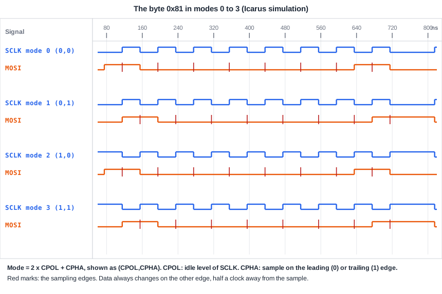
Mode 0 and mode 3 are by far the most common, and many devices support both, because both sample on the rising edge. The device's datasheet always says which modes it supports; the master must be configured to match.
A Transaction
The example slave has four registers. A transaction is two bytes with chip select held low: a command byte (bit 7 = 1 for a write, bits 1:0 the register number) and a data byte. While the master sends the command, the slave sends its ID, 0xA5:
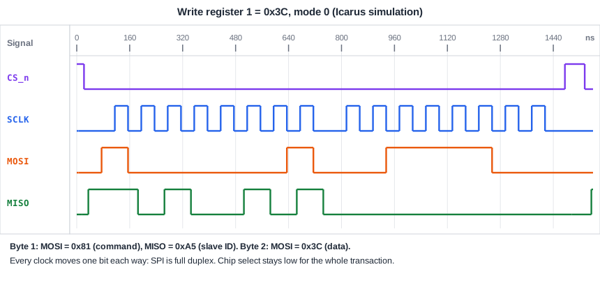
The same test runs in all four modes, with master and slave configured alike:
SPI mode 0 (CPOL=0, CPHA=0)
1535  write reg1 = 0x3c   (slave ID 0xa5)
3055  write reg2 = 0xc3   (slave ID 0xa5)
4575  read  reg1 = 0x3c   (slave ID 0xa5)
6095  read  reg2 = 0xc3   (slave ID 0xa5)
The other three modes print the same lines: the mode changes the waveform, not the data.
Quick Check
Q: In mode 0, why must the master put the first bit on MOSI before the first clock edge?
Show Answer
Because with CPHA = 0 the slave samples on the leading edge, which is the very first edge. There is no earlier edge on which the master could change the data, so the first bit has to be there when chip select goes low.
Running It in ChipVerify Lab
The example contains the SPI master, the register slave and this testbench. Change CPOL and CPHA in the testbench and compare the waveforms.
Common Mistakes
Mistake #1: Assuming every device uses mode 0
Each device chooses its mode. A master in the wrong mode samples on the wrong edge and reads every byte shifted by one bit.
Mistake #2: Releasing chip select between bytes
Many devices treat a chip select pulse as the end of a command. Hold CS_n low for all bytes of a transaction.
Mistake #3: Forgetting the bit order
SPI is usually MSB first, unlike UART, but some devices are LSB first. Check the datasheet.
Practice Exercise
Challenge: Mismatched Modes
Keep the master in mode 0 but configure the slave for mode 1 (CPHA = 1). Predict what the master sees, then run it.
Hint
The slave now changes MISO on the rising edge, the same edge on which the master samples, and expects MOSI to be stable on the falling edge.
Solution
SPI mode 0 (CPOL=0, CPHA=0)
1535  write reg1 = 0x3c   (slave ID 0x52)
3055  write reg2 = 0xc3   (slave ID 0x52)
4575  read  reg1 = 0x80   (slave ID 0x52)
6095  read  reg2 = 0x80   (slave ID 0x52)
The ID 0xA5 (10100101) arrives as 0x52 (01010010): every bit one place late, because the master samples just before the slave updates MISO. The writes went wrong too, so the reads return garbage. A one-bit shift in every byte is the typical symptom of a mode mismatch.
Open the ready-made example in the lab and run the simulation.
Summary
- SPI uses SCLK, MOSI, MISO and one active-low chip select per slave; the master drives the clock.
- It is full duplex: master and slave shift registers exchange contents, one bit each way per clock.
- CPOL is the idle clock level; CPHA selects sampling on the leading (0) or trailing (1) edge.
- Modes 0 and 3 sample on the rising edge and are the most common.
- Master and slave must use the same mode, bit order and chip select framing.
