
Standard SPI moves one bit per clock in each direction. For reading a serial flash, where a processor may fetch megabytes of code or data, that is the bottleneck. Dual and quad SPI reuse the data lines in both directions: two or four bits move per clock, in one direction at a time. This article explains how the extra lines are used, what a quad read looks like, and builds a quad SPI read master tested against a flash model.
8 min read | Intermediate
What You'll Learn
- Explain how dual and quad SPI use their IO lines
- Follow the phases of a quad read: command, address, dummy, data
- Calculate the read throughput of single, dual and quad modes
- Handle bidirectional IO lines in RTL
From Two Wires to Four
- Single SPI: MOSI and MISO, one bit per clock each way, full duplex.
- Dual SPI: MOSI and MISO become IO0 and IO1. In the data phase both carry data in the same direction: two bits per clock, half duplex.
- Quad SPI: two more lines, IO2 and IO3 (on flash chips usually shared with the write-protect and hold pins), give four bits per clock: a whole byte in two clocks.
Because every line can be driven by either side, each IO pin needs an output enable. The master releases the lines before the device starts driving them, which is one reason for the dummy clocks in a read command.
A Quad Read
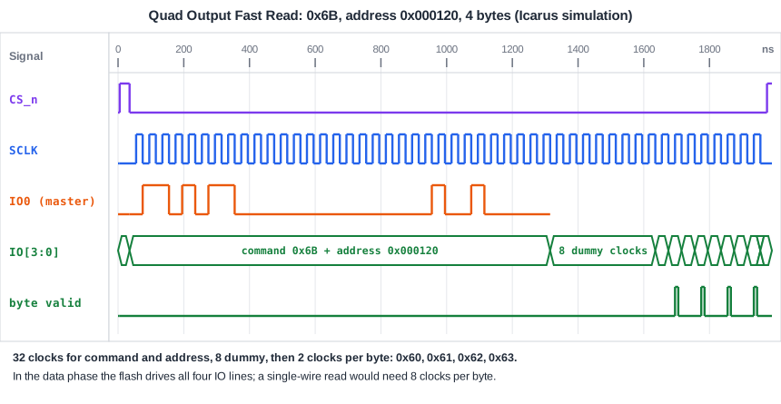
Serial flash memories have many read commands. A common one is Quad Output Fast Read, command 0x6B:
- Command: 8 clocks, 0x6B on IO0, MSB first.
- Address: 24 clocks, a 24-bit address on IO0.
- Dummy: 8 clocks with nobody driving, giving the flash time to fetch the data and turn the lines around.
- Data: 2 clocks per byte on IO0 to IO3, high nibble first, for as long as chip select stays low; the address increments automatically.
Other commands send the address in quad mode too (0xEB, Quad I/O Fast Read) or use only two lines (0x3B, Dual Output Fast Read). The command codes and dummy cycle counts vary between flash families, so the datasheet always decides.
The Master
The master counts rising SCLK edges. Up to edge 32 it drives the command and address on IO0, changing on falling edges as in mode 0. After edge 32 it releases IO0. From edge 41 on it samples a nibble on every rising edge and assembles bytes:
else if (!sclk) begin            // rising edge: the flash samples IO0, we sample data nibbles
  sclk  <= 1'b1;
  rises <= rises + 8'd1;
  if (rises >= 40) begin
    if (!have_hi) begin
      hi_nib  <= io_i;           // the high nibble comes first
      have_hi <= 1'b1;
    end
    else begin
      rdata      <= {hi_nib, io_i};
      byte_valid <= 1'b1;
      have_hi    <= 1'b0;
    end
  end
end
else begin                       // falling edge: put the next command or address bit on IO0
  sclk <= 1'b0;
  if (rises < 32)
    out_sh <= {out_sh[30:0], 1'b0};
  if (rises == 32)
    out_en <= 1'b0;              // command and address sent: release IO0
end
In the testbench, each IO line is a tri-state net driven by the master when its output enable is set, by the flash model in the data phase, and otherwise floating:
genvar k;
generate
  for (k = 0; k < 4; k = k + 1) begin : line
    assign io[k] = m_oe[k] ? m_o[k] : (f_oe ? f_o[k] : 1'bz);
  end
endgenerate
The flash model returns the low byte of the address plus 0x40 at every address. Reading four bytes from 0x000120:
1295  flash: command 0x6b, address 0x000120
1705  master read 0x60
1785  master read 0x61
1865  master read 0x62
1945  master read 0x63
Quick Check
Q: Why does the master stop driving IO0 after the address, eight clocks before the flash starts driving?
Show Answer
To avoid both sides driving IO0 at once. The dummy clocks give a safe turnaround: the master's driver turns off, then the flash's turns on, with time in between.
Throughput
A 4-byte read here took 32 + 8 + 8 = 48 clocks; a single-wire read with the plain 0x03 command would take 32 + 32 = 64. The gain grows with the length: in quad mode each byte costs 2 clocks instead of 8. A quad flash at 100 MHz streams about 50 MB/s, which is why processors can run code directly from quad SPI flash (execute in place) through a memory-mapped controller that turns bus reads into these commands.
Quick Check
Q: How many SCLK cycles does a 256-byte quad output read take, including command, address and dummy cycles?
Show Answer
8 + 24 + 8 + 2 x 256 = 552 cycles. The overhead of 40 cycles matters only for short reads.
Running It in ChipVerify Lab
The example contains the quad read master and the flash model. Change the address and the number of bytes.
Common Mistakes
Mistake #1: Wrong number of dummy cycles
Dummy cycles depend on the command, the device and often its clock frequency setting. With too few, the master samples before the data is there; with too many, every byte is shifted by a nibble.
Mistake #2: Forgetting to enable quad mode
Many flashes start with IO2 and IO3 working as write-protect and hold pins. A configuration bit must be set before quad commands work.
Mistake #3: Two drivers on an IO line
A master that keeps driving an IO line into the data phase fights the flash. Turn the output enable off before the turnaround.
Practice Exercise
Challenge: Eight Bytes
Set NBYTES to 8. Predict when the last byte arrives, then run it.
Hint
Each extra byte adds 2 SCLK cycles. With CLK_DIV = 2 on a 100 MHz clock, an SCLK cycle is 40 ns.
Solution
1295  flash: command 0x6b, address 0x000120
1705  master read 0x60
1785  master read 0x61
1865  master read 0x62
1945  master read 0x63
2025  master read 0x64
2105  master read 0x65
2185  master read 0x66
2265  master read 0x67
A new byte every 80 ns (two SCLK cycles), with the address incrementing inside the flash. The last byte arrives at 2265 ns, 320 ns after the fourth.
Open the ready-made example in the lab and run the simulation.
Summary
- Dual and quad SPI turn the data lines into bidirectional IO0 to IO3: 2 or 4 bits per clock, half duplex.
- A quad output read sends command and address on IO0, waits dummy cycles, then reads a byte every two clocks.
- Each IO line needs an output enable, and the dummy cycles give a safe turnaround.
- Command codes, dummy cycles and quad enable bits come from the flash datasheet.
- Quad SPI flash is fast enough for executing code in place.
