
Almost every peripheral has a bus slave: a small register block that software reads and writes through a bus. Its properties combine everything from this chapter: protocol assumptions for the bus master, read-after-write with a tracked address, and rules for special registers. This article checks an APB register block and finds an address decoder that lets writes to a read-only register land in another register.
10 min read | Intermediate
What You'll Learn
- Describe the APB protocol with assumptions on the bus master
- Check read-after-write for a register map with a tracked register
- Write rules for read-only registers
- Find an address decoding bug that corrupts a register
APB in Brief
APB, the Advanced Peripheral Bus of the AMBA family, is the simplest of the common on-chip buses. Every transfer takes two phases:
- Setup: the master raises
pselwithpenablelow, and drivespaddr,pwriteand, for a write,pwdata. - Access: in the next cycle the master raises
penable, with the same address and data. The transfer completes when the slave'spreadyis high.
For a slave under check, these master rules are assumptions:
m_access: assume property (@(posedge clk) disable iff (rst) psel && !penable |=> psel && penable);
m_stable: assume property (@(posedge clk) disable iff (rst) psel && !penable |=> $stable(paddr) && $stable(pwrite) && $stable(pwdata));
m_end:    assume property (@(posedge clk) disable iff (rst) psel && penable && pready |=> !penable);
m_setup:  assume property (@(posedge clk) disable iff (rst) penable |-> psel && $past(psel && !penable));
The Design: a Register Block
Four 8-bit registers: control at 0x0, data at 0x4, scratch at 0x8, and a read-only ID register at 0xC that always reads 8'hA5. The slave never inserts wait states:
module apb_regs (input clk, input rst,
                 input psel, input penable, input pwrite, input [3:0] paddr, input [7:0] pwdata,
                 output reg [7:0] prdata, output pready, output [7:0] ctrl);
  reg [7:0] r0, r1, r2;
  assign pready = 1'b1;                                  // no wait states
  assign ctrl = r0;
  wire wr = psel && penable && pwrite;
  always @(posedge clk)
    if (rst) begin
      r0 <= 8'd0; r1 <= 8'd0; r2 <= 8'd0;
    end else if (wr)
      case (paddr[3:2])
        2'd0: r0 <= pwdata;
        2'd1: r1 <= pwdata;
        default: r2 <= pwdata;                           // bug: a write to 0xC also lands in r2
      endcase
  always @(*)
    case (paddr[3:2])
      2'd0: prdata = r0;
      2'd1: prdata = r1;
      2'd2: prdata = r2;
      default: prdata = 8'hA5;
    endcase
endmodule
The write decoder uses default for the scratch register, so it also catches address 0xC. Software that writes the ID register by mistake, or a test that writes every address, silently changes the scratch register.
The Properties
- ID register: a read of 0xC returns
8'hA5. - Read after write: for a tracked register address
taother than 0xC, a read returns the last value written there.
`ifdef FORMAL
  // ... reset and the APB master assumptions in the lab form ...
  // the ID register always reads A5
  always @(*) if (!init && psel && paddr[3:2] == 2'd3) assert (prdata == 8'hA5);
  // read after write for a tracked register address
  (* anyconst *) reg [1:0] ta;
  reg [7:0] tv; reg tvalid = 1'b0;
  always @(posedge clk) if (rst) tvalid <= 1'b0; else if (wr && paddr[3:2] == ta) begin tv <= pwdata; tvalid <= 1'b1; end
  always @(*) if (!init && tvalid && ta != 2'd3 && psel && penable && !pwrite && paddr[3:2] == ta) assert (prdata == tv);
`endif
The example file contains the full set, including the master assumptions written in the lab form and an assumption that addresses are word-aligned.
The Counterexample
The run fails at step 6:
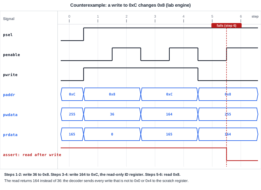
The tool writes 36 to the scratch register at 0x8 in steps 1 and 2, then writes 164 to the ID register at 0xC in steps 3 and 4, then reads 0x8 in steps 5 and 6. The read returns 164. The ID register itself still reads A5, so its own rule passes; the damage is in another register. Only a read-after-write rule over all addresses finds that.
Quick Check
Q: A register test writes and reads back each register in turn: 0x0, 0x4, 0x8, then reads 0xC. Does it find the bug?
Show Answer
No. It never writes 0xC between a write and a read of 0x8. The bug needs a specific order of accesses, which the formal tool finds without anyone thinking of it.
The Fix
case (paddr[3:2])
  2'd0: r0 <= pwdata;
  2'd1: r1 <= pwdata;
  2'd2: r2 <= pwdata;
  default: ;                                       // 0xC is read-only
endcase
With it, both properties pass. A good additional rule states the read-only behavior directly: a write to 0xC changes no register.
Quick Check
Q: Why are the APB master rules assumptions and not assertions here?
Show Answer
The block under check is the slave. The master is its environment, so the master's rules describe legal inputs. They become assertions when the master, or the bus interconnect, is checked.
Running It in ChipVerify Lab
The example below is the buggy register block with the master assumptions and both properties. It fails at step 6, within the free depth.
Common Mistakes
Mistake #1: Using default in a write decoder
A default branch that writes a register catches every unlisted address, including read-only and reserved ones. List every writable address explicitly and make default do nothing.
Mistake #2: Checking each register only against its own address
"Read 0x8 after writing 0x8" passes here. The tracked-address rule with the tool choosing the order of accesses catches writes that land in the wrong register.
Mistake #3: Leaving out the bus protocol assumptions
Without them, the tool drives penable without a setup phase or changes the address mid-transfer, and the slave fails in ways the bus never allows.
Practice Exercise
Challenge: Make 0xC Read-Only
Open the example and run it. Fix the write decoder. Then add a rule that a write to 0xC changes none of the three registers, and check it on both the buggy and the fixed design.
Hint
Look one cycle back: if the previous cycle was a write to 0xC, every register equals its previous value.
Solution
always @(posedge clk)
  if (!init && !$past(rst) && $past(wr) && $past(paddr[3:2]) == 2'd3)
    assert (r0 == $past(r0) && r1 == $past(r1) && r2 == $past(r2));
On the buggy design it fails at step 4, right after the first write to 0xC. On the fixed design it passes, together with the other two properties.
Open the ready-made example in the lab and run the formal check from the formal panel. The free tier allows a depth of up to 10 cycles, and PRO allows up to 100.
Summary
- A bus slave check combines protocol assumptions for the master, read-after-write with a tracked register, and special-register rules.
- APB master rules: setup then access, signals stable across the two phases,
penableonly after a setup cycle. - A write decoder with a writing
defaultlet writes to the read-only register at 0xC corrupt the scratch register, found at step 6. - The read-only register's own rule passed; only the read-after-write rule over all addresses saw the damage.
